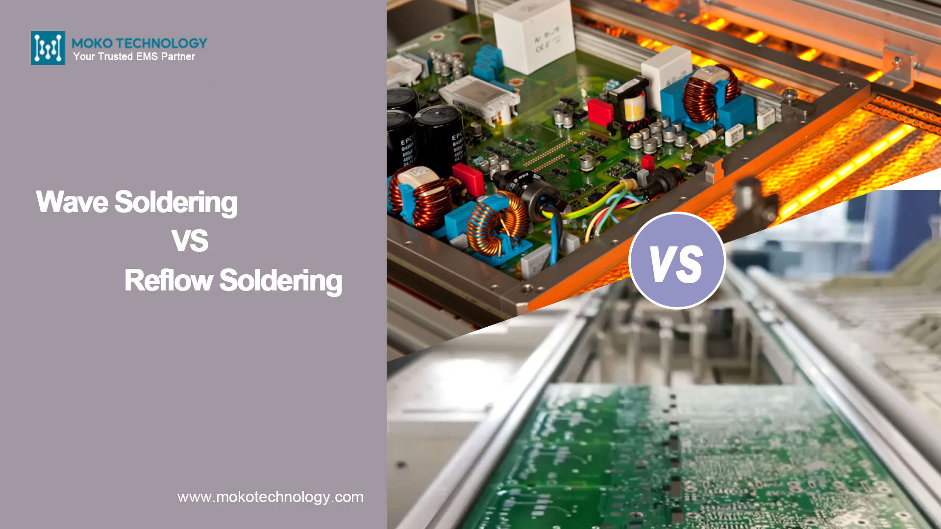
Soldering is a process of joining two metals by melting a filler metal, called solder, which flows into the joint and solidifies to form a strong bond. It is widely used in electronics manufacturing to assemble printed circuit boards (PCBs). There are two popular methods of soldering used in PCB assembly: wave soldering and reflow soldering, which play an important role in determining the performance of an electronic product. However, some people confuse them with each other and the difference between them seems vague. In this blog, we will compare these two methods and discuss their pros and cons.
What Is Wave Soldering?
Wave soldering is a soldering process that involves passing a PCB over a pan of molten solder. The pan of solder is typically made of an alloy of tin and lead, with a temperature range of 250-270°C. As the PCB passes over the pan, a wave of molten solder is generated, which wets the exposed metal surfaces of the components and the PCB, forming a strong and permanent bond.
Development History
Transistor was invented in 1946 by John Bardeen, Walter Brattain, and William Shockley at Bell Laboratories. This reduced the size of the electronic components. Some years later, lamination and etching were developed and this paved the way for a soldering technique that we could use at the production level.
Electronic components were mostly through-hole and it becomes impractical to solder them individually by using a soldering gun. There was a need for applying solder to the entire board at once. Hence wave soldering was developed which allowed for running over the entire board with a wave of solder paste.
The Wave Soldering Process
Wave soldering involves 4 steps and we will look at them one by one.

1. Flux spraying
Soldering performance mainly depends on the cleanliness of the metal surface. It also depends on the functions of the solder flux. It plays a vital role in seamless soldering operations. Major functions of solder flux are:
• Eliminating oxides from the metal surfaces of component pins and boards.
• Stopping secondary oxidation of circuit boards during the thermal process.
• Reducing surface tension of the solder paste.
• Proper transmitting of the required heat.
2. Pre-heating
PCBs travel through a heat tunnel in a pallet along a chain which is similar to a conveyor belt. It is necessary for activating the flux and carrying out pre-heating.
3. Wave soldering
When the temperature continues to rise, solder paste melts to become liquid. This results in a wave of solder which travels throughout the board and allows components to solidly bond with the board.
4. Cooling
The wave soldering profile is conformed to the temperature curve. The curve starts to plummet after the temperature reaches its peak in the wave soldering stage. This is known as the “cooling zone.” We can successfully assemble the board after cooling it to room temperature.
Pros of wave soldering
High throughput: Wave soldering is a high-speed process that can solder multiple components simultaneously, making it suitable for mass production.
Strong mechanical bond: The solder joint formed by wave soldering is strong and reliable, making it ideal for components that experience high mechanical stress.
Good thermal performance: The heat from the solder wave can penetrate the PCB, ensuring good thermal performance and heat dissipation.
Cons of wave soldering
Limited component compatibility: Wave soldering is not suitable for all PCB components, as some components may not be able to withstand the high temperature of the solder wave.
Limited precision: The solder wave cannot be precisely controlled, which may result in poor solder quality or damage to sensitive components.
Environmental concerns: The use of lead-based solder in wave soldering can pose environmental hazards, making it less desirable in some applications.
What Is Reflow Soldering?

In reflow soldering, components are first temporarily stuck to the pads on circuit boards. Then they are permanently glued together by hot air or other methods of thermal conduction and radiation. Reflow soldering is relatively easier to perform and even a novice can perform it easily on a small scale. Reflow soldering requires a reflow soldering machine which we often call a reflow soldering oven.
Reflow Soldering Process
As mentioned earlier, electrical components are temporarily attached to the contact pads before the soldering actually commences. This includes two steps. In the first step, solder paste is precisely applied to each pad via a solder paste stencil. In the second step, we use to pick and place machines for placing the components on the pads. Actual reflow soldering doesn’t start until the completion of these preparations.
The actual soldering process has four steps which we are about to discuss.

-
Pre-heating
Pre-heating is very important if you want to manufacture premium quality PCBs. It has two major purposes during reflow soldering.
- It allows PCB assembly to easily reach the required temperature and achieve the necessary thermal profiling.
- Pre-heating pushes out volatile solvent within the solder paste and helps in completely expelling them. If we don’t perform it correctly then it will affect the soldering quality.
-
Thermal Soak
Reflow soldering also depends on the flux which is contained in the solder paste. Hence, the temperature has to rise significantly so that the flux may activate. Otherwise, the flux won’t play an active role in the reflow soldering process.
-
Reflow Soldering
This step involves the peak temperature of the whole process. Peak temperature allows the melting and reflowing of the solder paste. Temperature control is very important in the reflow soldering process. If the temperature is very low then it can stop the solder paste from reflowing while if the temperature is very high then it may damage the board or SMT components.
For instance, BGAs have a lot of solder balls that melt during the reflow soldering. If we don’t achieve the optimal soldering temperature than these balls may melt unevenly and BGAs may suffer from rework.
-
Cooling
When we achieve the peak temperature, the temperature curve will start falling. Cooling leads to solidification of the solder paste and parts are permanently fixed to their contact pads on the board.
Pros of reflow soldering
High precision: Reflow soldering allows for precise control of the soldering process, resulting in high-quality and reliable solder joints.
Suitable for complex PCBs: Reflow soldering is suitable for complex PCBs with multiple components, as it allows for selective soldering of individual components.
Environmentally friendly: The use of lead-free solder in reflow soldering makes it a more environmentally friendly option.
Cons of reflow soldering
Limited throughput: Reflow soldering is a slower process than wave soldering, as each component must be individually soldered, which may not be suitable for mass production.
Sensitive to temperature: Reflow soldering is sensitive to temperature changes, and any variation can result in poor solder quality or component damage.
Limited mechanical strength: The solder joint formed by reflow soldering may not be as strong as that formed by wave soldering, making it less suitable for components that experience high mechanical stress.
To learn more about reflow soldering, check out our other blog: Reflow soldering on PCB
Difference between Wave Soldering and Reflow Soldering
We can never ignore the difference between reflow soldering and wave soldering because it is important when you are selecting PCBA services. A soldering modification tends to make drastic changes in the entire assembly manufacturing process. These include manufacturing cost, time to market, efficiency, gains, etc.
Soldering Process

The main difference between reflow soldering and wave soldering in terms of the manufacturing process is the flux spraying step. Wave soldering involves this step while reflow soldering doesn’t. We use flux for promoting the soldering process. It helps by playing a protective role by eliminating the surface tension and reducing surface tension. Flux only works when we activate it which we can only achieve through intensive time and temperature control. In reflow soldering, flux is present in the solder paste. Therefore, we need to appropriately arrange and achieve the required flux content.
Application
Generally, wave soldering works best for DIP and THT while reflow soldering is ideal for SMT assemblies. However, a circuit board rarely contains only through-hole components or surface-mounted devices. That is why we often have to use a mixture of SMT, THT, and DIP. When it comes to mixed assemblies, we first carry out SMT and then focus on DIP or THT. This is because the temperature of reflow soldering is much higher than the one in wave soldering. If we don’t follow this sequence then the solder paste might melt again. This can lead to well-soldered components falling from the board or suffering from defects.
Production Capacity
We use wave soldering mainly for mass production. It helps in manufacturing a large number of printed circuit boards in a relatively small amount of time. While reflow soldering is suitable for complex PCBs with high precision requirements. And we also use reflow soldering when we manufacture a small number of printed circuit boards. We avail of this technique when we don’t have very tight time constraints.
Below is a table listing differences between wave soldering and reflow soldering vividly:
| Aspect | Wave Soldering | Reflow Soldering |
| Process | Solder is in a molten wave or fountain | Solder paste is pre-applied, and components are reflowed in an oven |
| Suitable for | Through-hole components | Surface mount components |
| Component Handling | Limited component size and density | Suitable for smaller, densely populated PCBs |
| Solder Application | Applied to the entire PCB | Applied selectively to specific areas |
| Flux Application | Typically uses a separate fluxing stage | Flux is often included in solder paste |
| Heating Method | Convection heating from below the PCB | Radiant or convection heating in an oven |
| Temperature Control | Temperature is consistent throughout | Temperature profiles are carefully controlled |
| Control Complexity | Relatively simpler control | Requires precise temperature profiles |
| Reflow Atmosphere | Inert nitrogen atmosphere not commonly required | May use nitrogen atmosphere for specific applications |
| Process Time | Faster process due to simultaneous soldering | Longer process with separate preheating, reflow, and cooling phases |
| Inspection & Rework | Easier inspection and rework for through-hole components | Reworking surface mount components can be more challenging |
| Solder Waste | More solder waste due to the entire PCB being exposed | Less solder waste as solder paste is applied selectively |
| Equipment Size | Typically larger equipment | Smaller and more compact equipment |
| Cost | Generally lower equipment cost | Higher initial equipment cost |
Choosing the Right PCB Soldering Process
Reflow soldering and wave soldering are both effective methods for PCB assembly. The right option depends on several factors related to your specific boards and production environment. If the PCB primarily uses surface mount devices, reflow soldering is usually the best bet. The solder paste and heat profiling allow for precise soldering of small SMD components. However, if you mainly have through-hole parts, wave soldering excels at quickly flowing solder into the holes for fast assembly. For boards with both SMDs and through-hole parts, a hybrid approach with selective wave soldering and reflow may be optimal. Beyond component types, also consider production volumes, equipment investment costs, precision requirements, and operator experience. Reflow soldering provides tremendous precision but lower volumes, while wave soldering has higher throughput yet lower joint quality. Analyzing all these elements upfront prevents issues down the line. There’s no one universally superior process – choosing what’s best for your particular PCB design and production goals ensures high-yield, reliable soldering.
MOKO Technology, as a leading electronics manufacturer in China, we have a large manufacturing setup for making PCBs that has the capacity to perform both wave soldering and reflow soldering. On top of that, we have a large production capacity so we can easily perform any mix of soldering techniques for bulk orders. If you are looking for a reliable resource for performing soldering on your PCBs then feel free to contact us. We are hoping to hear from you soon!


