The electronic devices are advancing rapidly, they require compact designs and efficiency. Among many choices that matter, QFN packages is an all-time popular choice. What makes this type of package so popular? Should you use it in your projects too? This guide takes a clear and comprehensive look at it.
What Are QFN Packages?
QFN stands for Quad Flat No-leads. QFN packages attach silicon dies (the ASIC) to a printed circuit board (PCB). It is implemented using surface-mount technology. As the name suggests, this package did not include the classical leads that used to be there in the past. Instead of having usual leads, Quad flat no-lead packages have edge pads with an open solder pad under. This structure can improve electrical and thermal performance, and that’s why QFN packages are very popular among users.
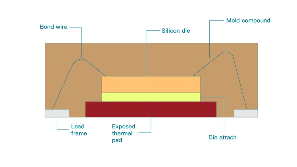
A QFN package generally consists of the following basic components:
Lead Frame: This part is very critical in determining the performance of the IC. It basically serves as the support for the package.
Single or Multiple Dies: These are actually the silicon chips inside the package and are mounted to the circuit board using the surface-mount technique.
Wire Bonds: These are usually made of copper or gold. These wires form the necessary connections between the lead frame and the dies.
Molding Compound: This material surrounds and protects the internal components. It provides electrical insulation, prevents corrosion, and strengthens the durability and reliability of the package.
Types of Quad Flat No-Lead Packages
- Air-cavity QFN: This type is characterized by a plastic or ceramic lid, a copper lead frame, and a body molded from plastic that isn’t sealed. This type is usually used in microwave systems that operate between 20 to 25 GHz, where an air cavity is necessary
- Multi-Row QFN Package: This type of design meets the requirements of a high number of pins by using multiple rows of pins, similar to BGA technology but often it is made at a lower price.
- QFN with Wettable Flanks: This type of quad flat no-lead package has exposed metal flanks or terminals on all four sides of the package body. All those flanks are designed to be wettable by solder and in this way, the solder will have the possibility of wicking up and making a strong solder connection between the package and PCB.
- Fc-QFN Package (Flip-Chip Quad Flat No Lead): It uses flip chip connections in a copper lead frame. And it is smaller than a regular QFP package and also makes the electrical performance better due to the fact that the electrical path is shorter.
- Wire bond QFN: In a wire bond QFN package, semiconductor die is mounted on a leadframe and, afterwards, wire bonds are used to connect the package terminals to the semiconductor die. This, of course, makes a smaller package footprint as opposed to regular Quad Flat Packages (QFPs) with exposed leads.
Punch Type QFN vs Sawn Type QFN
QFN packages may also be divided into two main types depending on the manufacturing process:
Punch type QFN: This style is produced with one mold cavity. After the molding process a special tool is used to punch out each individual package from the molded matrix. This method is very productive for mass production and usually results in a clean, sharp cut.
Sawn type QFN: On the other hand, sawed type QFNs are produced through the mold array process. This involves the process of making a large sheet of molded packages cut out into individual units using a saw. The technology is very efficient in managing large volumes.
Advantages and Limitations of QFN Packages
Advantages:
- Compact and has a low profile so it’s ideal for space-constrained applications in devices such as smartphones, wearables, and IoT devices.
- Better thermal dissipation due to the exposed die pad which allows thermal to be transferred more efficiently to the PCB.
- Higher thermal efficiency translates into better performance and reliability.
- Good for applications when size, weight, and power consumption are very critical factors.
Limitations:
- No external leads do not make it easy for visual inspection or rework of solder joints, which are hidden under the body of the package.
- For small pin pitch and a higher number of I/O, there is a higher risk of solder bridging, and the processes need to be very well controlled to avoid them.
- Not very ideal for some high-reliability purposes.
QFP vs. QFN: What Is the Difference? How to Choose Between Them?
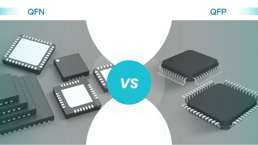
QFP and QFN are the two most common integrated circuit packages. Although their names differ only by one letter, the QFP package features gull-wing leads that protrude from the package body. This is very helpful when inspecting or reworking it, and at the same time, it is quite compact.
QFNs will have better thermal dissipation because the die pad is exposed, and this type of design enables more heat to be transferred to the PCB. However, QFNs are difficult to visually inspect and rework due to the fact that the solder joints will be buried under the package.
Consider the space in the board for the component, the need for thermal performance, and the capabilities of the manufacturing process. If the need is space and thermal performance, then QFNs might be the choice, but if ease of inspection and ease of rework is what is needed, then QFPs can be the better alternative.
Further reading: IC Package Types: How to Choose the Right One?
Applications of QFN Packages
QFN packages are especially popular in sectors where saving space and having top performance are of paramount importance. QFNs are used in the following sectors:
- Consumer electronics: The quad flat no-lead package is commonly used in smartphones and tablet PCs with general purposes of occupying a small footprint and having excellent heat management.
- Automotive Systems: High performance of QFN packages makes it a device used in vital modules such as engine control units.
- Communication Apparatus: QFNs find application in high-speed network devices where rapid signal processing is essential.
