Why would you not go for a solid copper filled via than a plated via?

Last week I send my PCB to the supplier for making trial samples and batch manufacturing. After their checking, they asked us whether choose solid copper filled via or a plated via. No idea to decide.

A solid, copper (not solder-filled) via is going to cost you a lot more money. Because it adds processes. Unless a via has too large a resistance.

Solder filling will improve resistance to some extent.

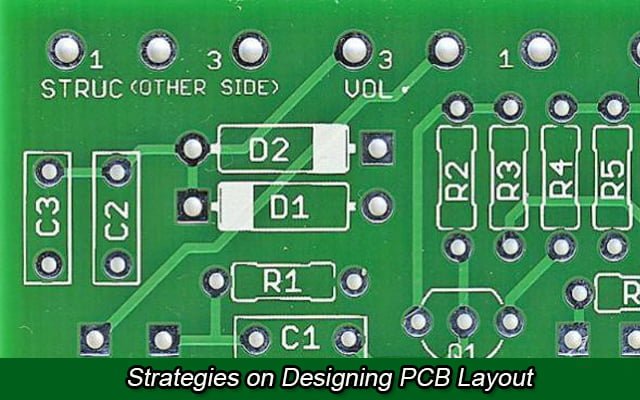
Read More: Design for Manufacturing

#PCB Design

Picture of Oliver Smith

Oliver Smith

Oliver is an experienced electronics engineer skilled in PCB design, analog circuits, embedded systems, and prototyping. His deep knowledge spans schematic capture, firmware coding, simulation, layout, testing, and troubleshooting. Oliver excels at taking projects from concept to mass production using his electrical design talents and mechanical aptitude.

What Others Are Asking

Read Detailed Advice From Blog Articles

The Ultimate Guide to PCB Layout Design
Ryan Chan

The Ultimate Guide to PCB Layout Design

PCB layout design is a key step in the manufacture of circuit boards. A reasonable PCB layout is conducive to controlling the production cost and

Strategies on Designing PCB Layout
Ryan Chan

Strategies on Designing PCB Layout

Why PCB Layout is Needed We use Printed Circuit Boards (PCB) for connecting electronic components by using conductive tracks. This allows for prototyping electric circuits

Scroll to Top