Why are there no BGA chips with triangular tessellation of circular pads?

A triangular tiling would allow π⁄√12 or 90.69% of the footprint to be reserved for the solder balls and the surrounding clearance, while the ubiquitous square tiling only allows π/4 or 78.54% of the footprint to be used. Why are there no BGA chips with triangular tessellation?

Unless you use via-in-pad, which costs more, you need room to put routing vias in between the pads.

Read More:  Typical Error Categories for BGA PCB Soldering Joints

#PCB Assembly #PCB Design

Picture of Oliver Smith

Oliver Smith

Oliver is an experienced electronics engineer skilled in PCB design, analog circuits, embedded systems, and prototyping. His deep knowledge spans schematic capture, firmware coding, simulation, layout, testing, and troubleshooting. Oliver excels at taking projects from concept to mass production using his electrical design talents and mechanical aptitude.

What Others Are Asking

Can I make a PCB without a ground plane?

Recently we are developing a portable device which should be very tiny and light. In terms of PCB design, I am thinking whether it is a good idea to exclude ground plane to minimize the product size.

What kinds of test is suitable for low volume PCB order?

I’ve ordered fabrication and assembly of small PCB batches (100pcs) a couple of times already. Each time the factory asked me if I want to do test on the PCB. But I don’t what to do about it. And I test them by myself. Then, the result of the testing is unacceptable with 15% soldering problems. So bad. I think I will ask the supplier to test them before delivery.

Read Detailed Advice From Blog Articles

Strategies on Designing PCB Layout
Ryan Chan

Strategies on Designing PCB Layout

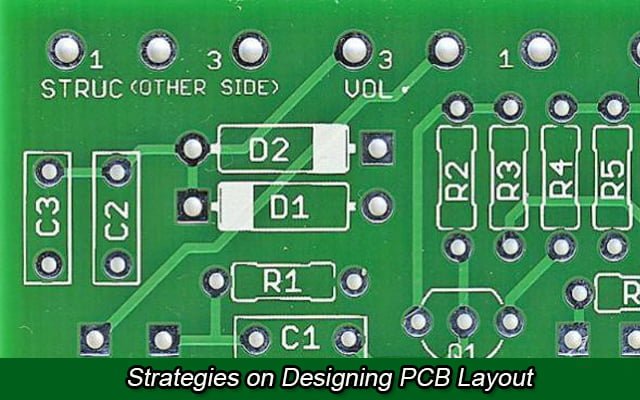
Why PCB Layout is Needed We use Printed Circuit Boards (PCB) for connecting electronic components by using conductive tracks. This allows for prototyping electric circuits

Scroll to Top