Flawless PCB soldering is imperative for proper functioning of a printed circuit board. However, even experienced technicians can make small mistakes that lead to soldering defects. One common issue is solder bridging, which can cause short circuits and other problems that impair the PCB’s performance. Properly addressing solder bridges is crucial for assembling high-quality PCBs that function as designed. In this article, we will explore what a solder bridge is, what causes it, how to prevent it, and how to fix it if it occurs. Read on to learn key tips for understanding and preventing this important soldering defect.
What Is a Solder Bridge?
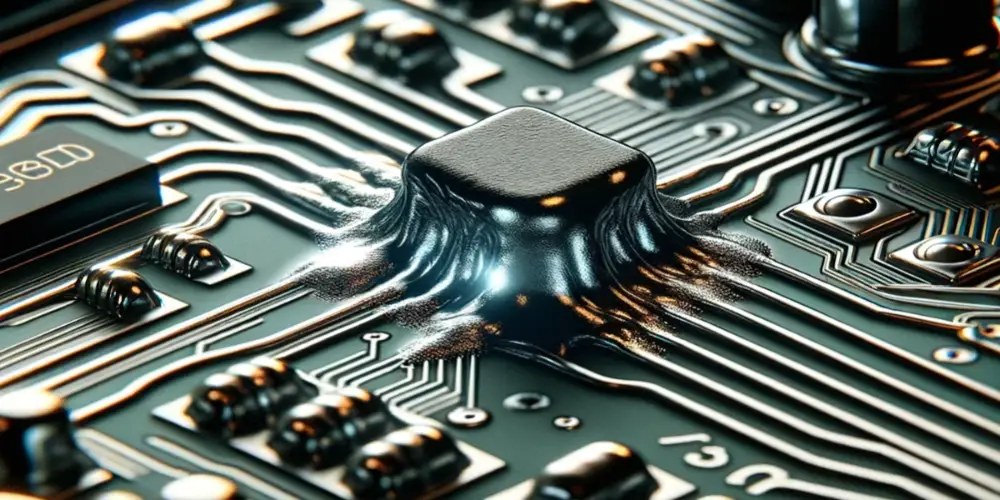
A solder bridge is an unintended electrical connection between two conductors on a printed circuit board that occurs due to excess solder. When too much solder is applied, it can form a “bridge” between adjacent PCB traces, pads, or components that are meant to remain electrically isolated. This causes an unwanted short circuit between the two points.
Solder bridges can form between the leads of a component, between two traces, or between pads and traces. The excess solder builds up, rising above the PCB surface to create a bridge between the conductive elements. This bridge allows current to flow between points it shouldn’t, which can lead to circuit failure. Solder bridges are often microscopic in size and hard to detect visually. But they can cause a range of problems from simple malfunctions to damaging short circuits.
What Causes PCB Solder Bridge?
Solder bridging can result from both manufacturing processes and PCB design decisions. Key causes include:
- Excessive solder paste deposit – Too much solder paste applied to pads can lead to bridging during reflow. This may be due to incorrect stencil design, poor stencil alignment, or excessive print pressure.
- Insufficient solder mask between pads – Lack of solder mask to electrically isolate adjacent pads allows solder to bridge between them. Proper mask definition is needed.
- Pad spacing too narrow – Pads spaced too closely together increases bridging risk. Minimum spacing rules must be followed.
- Misalignment – Poor alignment of stencils or components can lead to solder paste or leads bridging pads. Precise alignment processes are required.
- Residues – Flux residue or other contaminants on PCBs or stencils can cause solder to bridge between pads. Regular cleaning is essential.
- Insufficient preheat – Low preheat temperatures can prevent solder paste from properly liquefying, increasing bridging. Adequate thermal ramps are needed.

Measures to Prevent Solder Bridges
Fortunately, there are many feasible methods to prevent the occurrence of solder bridges. Let’s explore some of the key ones:
Use Optimal Lead Lengths for Through-Hole Components
The leads of through-hole components that are too long can lead to solder bridges between adjacent pins. To prevent this, research and use the ideal lead lengths for your PCB thickness, component size, soldering method, etc. Consult your PCB assembly provider for guidelines.
Follow Recommended Hole and Pad Sizes
Oversized holes and pads for through-hole parts decrease the spacing between pins, raising the risk of solder bridges. Refer to component datasheets for the proper hole diameter and pad size. This ensures adequate spacing between adjacent solderable surfaces.
Design for Maximum Manufacturing Reproducibility
It’s important to ensure that both surface-mount and through-hole components are designed with manufacturing convenience in mind. Follow IPC guidelines that define Level A as the preferred spacing and dimensions for reproducibility. Avoid unnecessarily small components or gaps unless required.
Apply Solder Mask Properly
Solder mask coating prevents solder adherence where not desired. Apply solder mask thoroughly between all component pins. Missing solder mask raises the chance of solder bridging during assembly.
Use Fiducials for Precise Component Positioning
Fiducial markers on the PCB enable accurate automated part placement. Follow IPC guidelines for optimal number and placement of fiducials. Poor fiducials increase misalignment and solder bridging risks.
Partner with a High-Quality Assembly Provider
A competent contract manufacturer is critical since assembly factors heavily influence solder bridging. Select a provider willing to discuss processes in detail. Inquire about stencil design, inspection protocols, etc. to understand their diligence in preventing solder bridges.
How to Address Solder Bridge Issues?
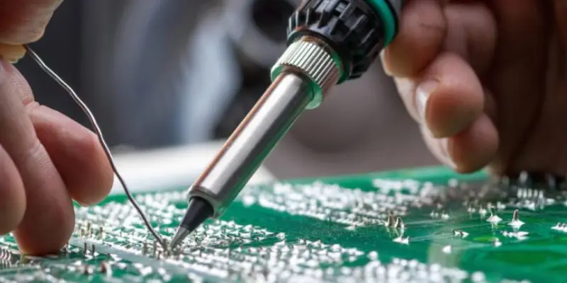
Dealing with soldering bridges poses a challenge for both seasoned and amateur electronics enthusiasts. Rest assured, if this issue arises, there are ways to rectify it. Here is a step-by-step guide:
Step 1: Set the temperature on your soldering iron to 150°C. Allow the iron to fully reach this temperature, which usually takes 20-80 seconds depending on the wattage and design of the iron.
Step 2: Visually inspect the circuit board to identify exactly where the solder bridge is located. You may need magnification to see small bridges clearly. Mark the location if needed.
Step 3: Place solder wick directly on top of the solder bridge. Press the hot soldering iron tip firmly onto the wick. The application of heat induces the melting of solder, which subsequently gets absorbed into the copper braid. Maintain pressure until all the bridged solder absorbs into the wick.
Step 4: Reheat each of the contact points that were previously bridged one at a time with the iron. Apply a small amount of fresh solder to each contact point to form a new, solid solder joint separated from the other.
Step 5: Carefully wipe off any excess solder stuck to the tip of the still hot iron by wiping on a wet sponge or damp cloth. This keeps the tip clean for future use. Avoid touching the hot tip.
Step 6: Use a multimeter on the continuity setting to test connectivity across the points that were bridged. Place one probe on each point. A numerical reading indicates successful disconnection.
The Bottom Line
Soldering can be tricky, but utilizing proper techniques and tools will ensure defect-free results. Implementing key measures to avoid solder bridges is critical for any electronics project.
As your PCB and electronics manufacturing partner, MOKO Technology has expertise in PCB assembly, Our engineers continuously hone best practices for flawless PCB population and soldering. Contact us today to get started on your next electronics project!