What Are PCB Pads? What Are Their Functions?


In the manufacturing process of PCBA, soldering is a very important process, which is used to achieve the electrical connection between all components and the printed circuit board. And PCB pads play a crucial role in the PCB assembly process as they determine where the component will be soldered onto the board. Their sizes, shapes, and positions will affect the functionality and reliability of PCBA. Therefore, in today’s blog, we will take a closer look at PCB pads.
What Are PCB Pads?
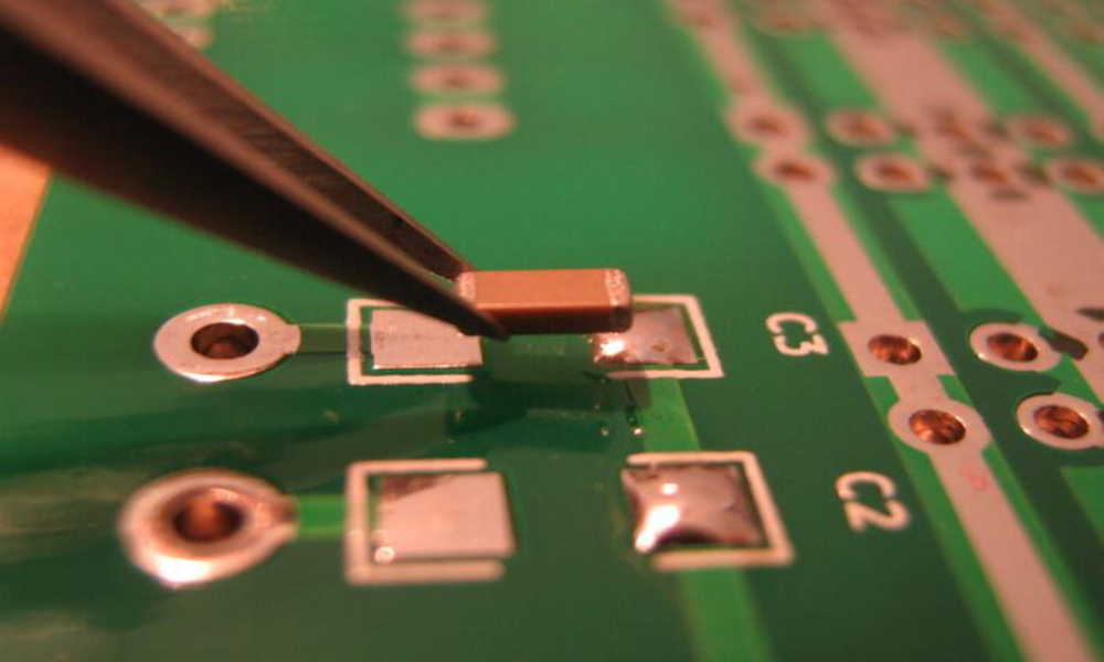
PCB pads, also known as soldering pads or solder pads, are areas on a printed circuit board that are specifically designed for the attachment of electronic components. These pads are typically circular or rectangular in shape and are made of copper or another conductive material. PCB pads serve as the connection points between the electronic components and the traces on the PCB. They provide a surface onto which the leads or terminals of the components are soldered or mounted. The pads are usually located at the endpoints of the traces, where components are intended to be placed. The design and placement of pads can directly impact the solderability, reliability, and thermal conduction of components.
Types of PCB Pads


PCB pads can be categorized into two main types based on the components and packaging methods: through-hole pads and surface mount pads.
Through-hole Pad
Through-hole pads are utilized for mounting through-hole components on a circuit board. These pads feature via holes where the pins of the components are inserted during the PCB soldering process. By soldering components via through-hole pads, durable solder joints are established, ensuring a dependable long-term mechanical and electrical connection to the PCB. However, it’s important to note that due to the presence of component leads and the necessary holes, the availability of routing space on a multilayer PCB may be restricted.
Surface Mount Pad
Surface mount pads are used for mounting electronic components directly onto the surface of a circuit board. Unlike through-hole pads, which require the components to pass through holes in the board, surface mount pads are designed for smaller components that can be soldered directly to the board’s surface. Surface mount pads offer several advantages. They enable a higher component density, allowing more components to be placed in a smaller space on the board. This compact arrangement enhances the functionality and performance of the circuit. Additionally, surface mount pads are particularly beneficial for the design of complex multi-layer boards, where space optimization is critical. However, it’s important to note that surface mount pads may not be suitable for components that generate significant amounts of heat. The compact nature of surface mount technology may restrict the dissipation of heat, potentially leading to overheating issues.
BGA (Ball Grid Array) pads belong to the category of surface mount pads, which are typically smaller and more densely packed than pads used for other surface mount components. And two types of BGA pads are commonly used:
- Solder Mask Defined Pads (SMD)
SMD pads for BGA components are designed with solder mask apertures that are smaller than the diameter of the pads they cover. This is intended to minimize the size of the pad that the component will be soldered to. By applying the solder mask to cover a portion of the copper pad underneath, two advantages are achieved: Firstly, it helps secure the pads to the circuit board, preventing them from lifting off due to mechanical or thermal stress. Secondly, the openings in the mask provide a guide for each ball on the BGA to align with during the soldering.
- Non-Solder Mask Defined Pads (NSMD)
Non-Solder Mask Defined (NSMD) pads are a type of copper pad used in printed circuit boards that are not covered by the solder mask. They are often smaller in size compared to the diameter of the solder ball, typically reducing the pad size by around 20% of the ball diameter. This reduction in pad size allows for closer spacing between pads, enabling more efficient routing and making them suitable for high-density and fine-pitch BGA chips. However, NSMD pads have a higher susceptibility to delamination, which can occur due to thermal and mechanical stresses.
The Size and Spacing of the PCB Pad
The size, shape, and spacing of the pads depend on the specific requirements of the components being used. Different types of components may have different pad configurations. For single-sided pads, the diameter or minimum width is 1.6mm; for double-sided weak-line pads, it is only necessary to increase the aperture of 0.5mm, because too large pad size will easily cause continuous welding. For pads with apertures larger than 1.2mm or pad diameters larger than 3.0mm, we should consider designing them as special-shaped pads. In addition, we need to know that the inner hole of the pad is generally not less than 0.6mm, because the hole smaller than 0.6mm is not easy to operate when punching.
As to the spacing of pads, it is important to consider the size of the component pins that will be inserted or attached to the pads, while also taking into account the related component package. Different components have varying requirements for the spacing of the pad mounting holes. For instance, when dealing with axial components with pin diameters less than 0.8mm, the installation hole pitch is typically 4mm longer than the standard hole pitch. On the other hand, if the pin diameter of an axial component exceeds 0.8mm, the installation hole pitch is generally more than 6mm longer than the standard hole pitch of the component body. When it comes to radial components, the mounting hole spacing should match the spacing between the component pins.
Problems Caused by Wrong PCB Pad Sizes
The size, position, and shape of solder pads in a printed circuit board footprint directly impact the manufacturing process of PCBs. Using incorrect solder pad sizes or improper placement can result in various issues during soldering in PCB assembly. Here are some problems you may encounter:
- Insufficient solder wetting
A pad size that is too small does not provide enough surface area for proper solder wetting, which can lead to poor solder joints and weak electrical connections.
- Solder bridging
When solder pads are too close together or improperly positioned, there is a higher risk of solder bridging. This occurs when molten solder unintentionally connects adjacent pads, causing short circuits.
- Tombstoning
In surface-mount component placement, tombstoning can occur when one end of a component lifts off the pad during soldering, resulting in an uneven or incomplete connection. This can happen if the pad sizes or positioning are incorrect, causing imbalanced thermal profiles during reflow.
- Solder wicking
Solder wicking can pose challenges to the construction of through-hole pads if they are not properly designed. When the drill size used for the lead is too large, the solder mask can wick down through the hole before establishing a solid connection. Conversely, if the drill size is too small, inserting the component lead becomes difficult, leading to slower assembly processes. It is important to find the right balance to ensure reliable and efficient through-hole connections.
- Incomplete solder joints
Insufficient spacing between small or closely spaced solder pads can restrict the formation of adequate solder fillets and solder alloy. This limitation may result in either a lack of solder joint formation or improper solder connections for the component.
- Solder voids
Large or irregularly shaped solder pads can contribute to the formation of solder voids or air pockets within the solder joint. These voids can weaken the joint and adversely affect thermal dissipation and electrical conductivity.
Conclusion
The quality of PCB pads plays a crucial role in the PCBA process and directly impacts the soldering quality of components on the circuit board. Understanding the importance of pads in PCB and PCBA manufacturing is essential. Choosing a reliable PCBA company is vital to ensure high-quality pads and soldering. MOKO Technology, a Chinese PCB manufacturer with 17 years of experience, offers comprehensive one-stop manufacturing services. Our services include PCB design, manufacturing, prototyping, component procurement, PCB assembly, and testing. Partnering with us can alleviate your concerns about quality issues, allowing you to focus on other aspects of your project.
Recent Posts
Impedance Matching: A Critical Factor in High-Speed PCB Design
Impedance matching has become a cornerstone of the signal integrity in the realm of high speed PCB…
How to Clean a Circuit Board Safely and Effectively?
It is important to learn how to clean a circuit board properly if you’re working…
Counterbore vs Countersink: Which to Choose for Your PCB?
When designing PCBs, selecting the appropriate type of holes for fasteners is crucial. And much…
PCB Copper Foil: Types, Properties & How to Choose
PCB copper foil is one of the most critical materials in the printed circuit board…
MOKO Technology Launches Vietnam Manufacturing Base in February 2025
Shenzhen, China - February 11, 2025 - MOKO Technology, a leading global electronics manufacturing service…
PCB Solder Mask: What It Is and Why Every Circuit Board Needs It?
While most people focus on the components and copper traces that make up PCBs, there's…


