Modern yüksek teknoloji dünyamızda, cihazlar sürekli olarak ileri geri sinyal gönderiyor. Herhangi bir komutun gerçekten gerçekleşmesi için, iki veya daha fazla devre kartı arasındaki iletişim önemlidir. Without a way to connect them, none of this instantaneous cross-talk would be feasible. This is where PCB gold fingers come in – they act as the connecting contacts that let mainboards and components like graphics cards or sound cards talk to each other. It’s a huge step forward from older electronics, where modules tended to be separate islands that didn’t interact smoothly. Gold fingers enable one circuit board to immediately understand the processes happening on another. Bu makalede, we’ll look at PCB gold fingers from different aspects. Let’s get started with the definition.
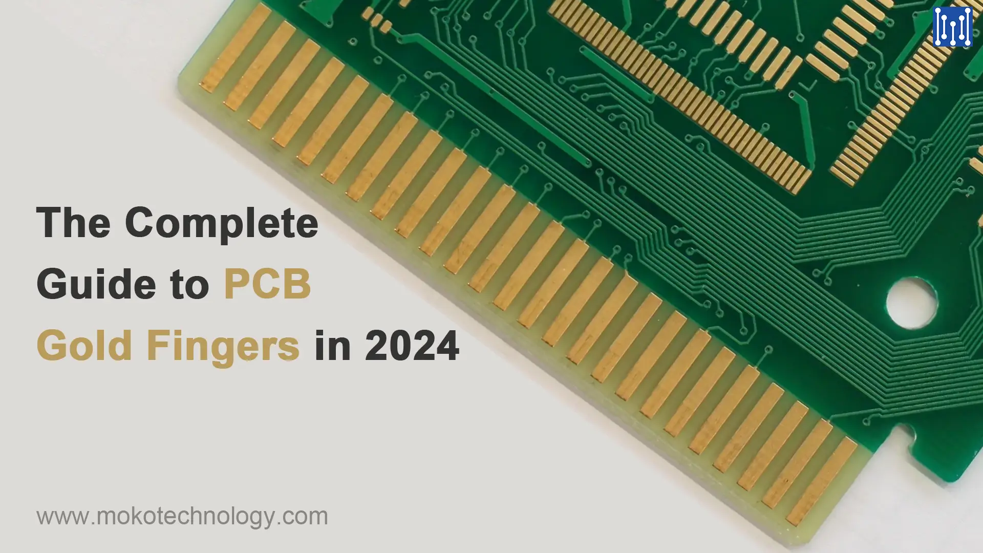
What Are PCB Gold Fingers?
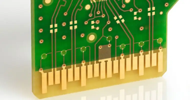
Gold fingers refer to the gold-plated connectors running along the edges of a printed circuit board. Their purpose is to allow a secondary PCB pano to interface with the motherboard of a computer or device like a smartphone. Since gold is highly conductive, it is used for the contact points on the board that need to transmit signals. esasen, gold fingers on PCB serve as bridges enabling different chips and components to communicate through established protocols. Critical functions like WiFi, Veri deposu, and processors all depend on clear channels between computer chips and circuit boards to carry out instructions.
There are two main surface treatment methods for gold fingers:
Akımsız Nikel Daldırma Altın (KATILIYORUM) -It stands out as a widely adopted gold finger method due to its cost-effective process that enables viable soldering The downside is that it results in thinner, softer surfaces prone to wear from repeated connections.
Electroplated Hard Gold – Allows for much thicker gold films (etrafında 30 microns typically) but is more expensive to manufacture. This type is reserved for specialty applications where durability is critical.
Types of Gold Finger PCBs
Gold fingers on printed circuit boards come in a few main types:
- Regular gold fingers (also called flush gold fingers): These are rectangular lehim pedleriof uniform length and width, neatly arranged along the edge of the board.
- Segmented PCB gold fingers(also called intermittent gold fingers): The solder pads here are rectangular but can be different lengths, located on the board edge. They have a disconnected section at the front.
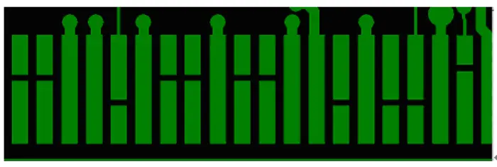
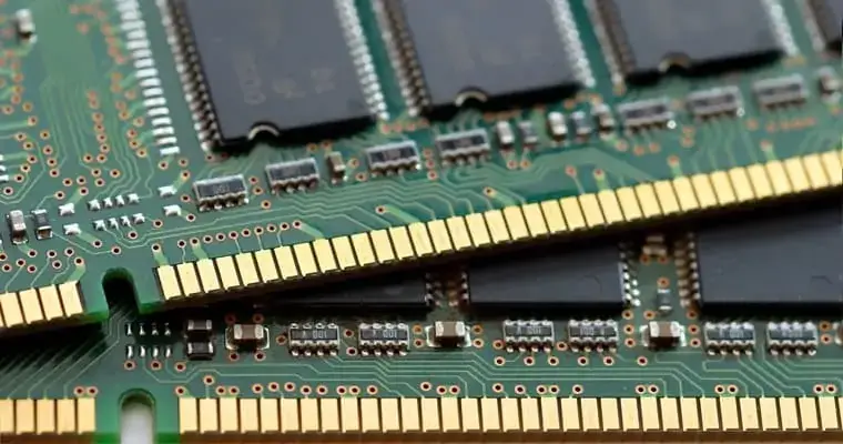
- Long-short gold fingers (also called uneven gold fingers): These are rectangular pads of different lengths along the board’s edge, often referred to as long-short gold fingers or uneven gold fingers. You’ll often find this type used for connections in memory modules, USB drives, card readers, vb.
Common Uses of PCB Gold Fingers
PCB gold fingers have a variety of common uses that enable connections between components in computers and other devices. Here are some of their most widespread applications:
- Interconnection points – Secondary PCBs connect to the main motherboard through female slots like PCI, ISA or AGP. The gold fingers in these slots transmit signals between peripheral devices/cards and the computer itself.
- Special adapters – PCB gold finger connectors enable numerous performance add-ons for personal computers through perpendicular expansion cards that slot into the motherboard. This allows enhanced graphics, sound, vb. Since these adapter cards rarely detach, the gold fingers tend to outlive the cards.
- External connections – Peripherals added to a computer station, like speakers, scanners and printers, plug into specific slots on the back of the tower. These ports connect to PCBs that then interface with the motherboard through gold fingers.
For any connected device to function, its own circuit board needs power. The gold fingers and slots on the motherboard facilitate this power transfer. They essentially empower modular PCBs to operate and provide functionality to both stationary and portable computing products.
PCB Gold Finger Beveling
Beveling of the gold fingers is an important process, as it optimizes them for easier insertion and better connectivity. The beveled shaping and layered plating are key to producing gold fingers that can reliably interface with ports and slots. On printed circuit boards, PCB gold finger plating is done after the solder mask application but before the final surface finish. The primary steps in the plating procedure are:
pah kırma – The edges of the gold fingers are beveled at angles of 30-45 degrees typically. This angled shaping makes it easier for the fingers to insert into their matching slots and connectors.
Altın kaplama – One to two microns of hard gold is plated onto the nickel. Cobalt is often added to the gold to reduce surface resistance.
Nickel Plating – İlk, three to six microns of nickel are plated onto the connecting edges of the fingers as a base layer.
Design Rules of PCB Gold Fingers
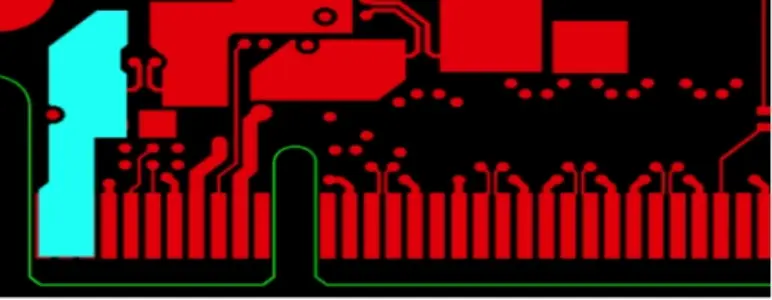
- Keep plated through holes away from the fingers by at least 1mm. Plated through holes require copper plating around the hole on all layers. This copper can flow onto the gold fingers during plating and cause contamination or plating thickness issues. Maintaining a 1mm keepout prevents this.
- Maintain spacing between the fingers and any solder mask or silkscreen printing. This prevents material from overflowing onto the fingers during application which can interfere with insertion.
- Orient the fingers on the side of the board opposite from the component center. This aids in insertion and alignment as it clears components on the bottom side.
- Do not place any SMD parts, deliklerden kaplama, or solder pads within 1mm of the fingers. This prevents interference with the interfacing connector.
- Remove all inner layer copper beneath the fingers, typically 3mm beyond the edge of the finger width. This prevents inner layer copper from being exposed during PCB beveling/chamfering which looks bad aesthetically.
- Limit the maximum finger length to around 40mm. Longer fingers are prone to damage during handling and insertion.
- Avoid soldermask or silkscreen printing in areas immediately adjacent to the fingers where material can overflow causing buildup issues.
- Design continuous openings in the solder mask around the fingers. This prevents the need for score lines or steel mesh.
Standards of Circuit Board Gold Fingers
The Association Connecting Electronics Industries IPC provides standards for the design and fabrication of printed circuit board gold fingers. These guidelines have evolved over time through various IPC publications.
The key aspects of PCB gold finger standards include:
Gold Plating Composition – To maximize durability, the gold plating should incorporate 5-10% cobalt. This increases hardness along the contacting edges.
Kaplama kalınlığı – Acceptable gold plating thickness ranges from 2 için 50 microinches. Thinner platings around 2-3 microns are often used for prototypes. Thicker platings of 5-10 microns provide longer life for high insertion cycles.
Görsel İnceleme – Gold fingers should exhibit a smooth, clean finish under magnification with no visible contaminants or nickel.
Adhesion Testing – An adhesive tape test can validate proper plating adhesion. No gold residue should be visible on the tape after application and removal from the fingers.
MOKO Technology'de çalışıyor, we’ve been producing printed circuit boards for almost 20 yıllar. In that time, we’ve honed our skills in all aspects of PCB üretimi – from rapid prototypes to medium and small production runs. One area we excel at is manufacturing high-quality gold fingers on circuit boards. We follow industry standards closely to ensure the gold plating has the right hardness and adhesion. If you have any questions about our gold finger fabrication capabilities, lütfen buraya tıklayın to contact us.