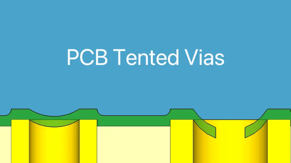
PCB vias refer to small holes that are drilled on the PCB with the intention of creating an interconnection between different layers on the board. While PCB vias are crucial for the overall functionality of circuit boards, there are issues associated with them, including their vulnerability to contaminants as well as the possibility of developing solder bridges during the assembly stage. This is where PCB via tenting comes in handy. Via tenting involves using a solder mask that shields the via holes to avoid the flow of solder into them during the soldering stage. In this article, we are going to learn about its benefits, tented via techniques, and design consideration.
What Is PCB Via Tenting?
PCB via tenting is one of the procedures in which portions of vias are covered or can be said to be tented. Vias are plated through holes in the PCB with small apertures that provide electric connections between layers of the PCB and are usually exposed on the surface of the PCB. The reason for the use of via tenting is to ensure that these vias are shielded physically to avoid some unprotected conditions which may occasion certain environmental or electrical disasters. Applying a material that conforms like solder mask, epoxy or polyimide covers the exposed metal surfaces of the vias and thus insulates them.
Benefits of PCB Via Tenting

Protection from Contamination
PCB via tenting helps protect the via holes from situations such as dust, moisture, and other contaminants from the environment. This protection is indeed essential in order to reduce the chances of corrosion and to guarantee long life of the PCB.
Prevention of Solder Bridging
Covering the vias with a solder mask could also protect the vias from the solder flow in the subsequent assembly process. This minimizes the chances of solder bridges forming over the joints to improve the electrical connection as well as minimize on the chances of solder forming a bridge over other areas leading to shortening or other forms of defects.
Enhanced Electrical Performance
Tenting plays a role of protecting the vias from being damaged by contaminants and solder since it covers the desired conductive pathways. This leads to more uniform electrical behavior, which translated into better performance over equally higher frequencies.
Improved Thermal Management
Although tenting can have a minor effect on thermal dissipation, at the same time, it aids in pinpointing out the necessary thermal characteristics of the PCB and thus offers an added layer of protection. This is especially necessary in such application areas as high voltage and current where heat dissipation is paramount.
Enhanced Mechanical Strength
The solder mask also has mechanical benefits: it shields the vias and makes them more resistant to any mechanical strain that a circuit board may be subjected to during assembly.
Different Tented Via Techniques
| Complete Tenting
| This technique is meant to coat the top and bottom layers of the PCB with solder mask, which can effectively protect the via from other elements and provide the best insulation for it.
|
| Partial Tenting
| When partial tenting is employed, only one of the layers of the PCB is coated with the solder mask while the other side is left exposed; it is especially useful where thermal dissipation through the via is required or where access is required.
|
| Tenting with Coverlay
| This technique involves using of Coverlay, a flexible dielectric material rather than a solder mask; rigid-flex or flexible PCBs are generally manufactured from this material.
|
| Tenting with Cap Plugging
| This method involves covering the via with a layer of solder mask first and then filling it with a non-conductive material like resin or epoxy to encapsulate the entire via. As a result, it enhances protection against environmental forces and mechanical stresses.
|
| Tenting with Copper Fill
| When forming a via under a layer of solder mask, rather than having the via practically empty, copper fill can be used thus supplementing the via’s structural support as well as thermal capabilities.
|
| Via Plug
| Besides applying a solder mask to the via it is also possible to fill the via with conductive or non-conductive material to close it up; this form is more commonly used in high density interconnect PCBs where space is critical.
|
Design Considerations for Tented Via
Solder Mask Type and Material
Solder mask type and material are another crucial factor required to be considered while designing tented vias. The solder mask material of the PCB should be compatible, and the choice of using a liquid photoimageable (LPI) solder mask or a dry film solder mask can be chosen for the PCB.
Via Size and Aspect Ratio
The diameter of the via and its aspect ratio (depth-to-diameter ratio) is another important factor to consider. In general, the smaller the via is in diameter, the easier it is to tent; and the aspect ratio must be within the manufacturing capabilities.
Pad Size and Clearance
Designers should leave enough pad diameter around the via and make sure that there is suitable space between the fabricated via and other pads or lines to avoid any mask misalignment.
Placement and Density
These vias should not be kept too close to the components or any other vias because mask adhesion is a problem, and also, the densities of the vias should not also be too high in order to control possible difficulties of a uniform application of the solder mask.
Electrical Performance
The impact of tented vias on signal integrity, particularly in high-frequency circuits, should be assessed, considering whether tenting will affect the via’s electrical characteristics such as capacitance.
Thermal Management
The impact of tenting through holes or vias on controlling thermal management of the PCB should be determined in order to avoid any improper orientation of thermals vias or heat sinks


