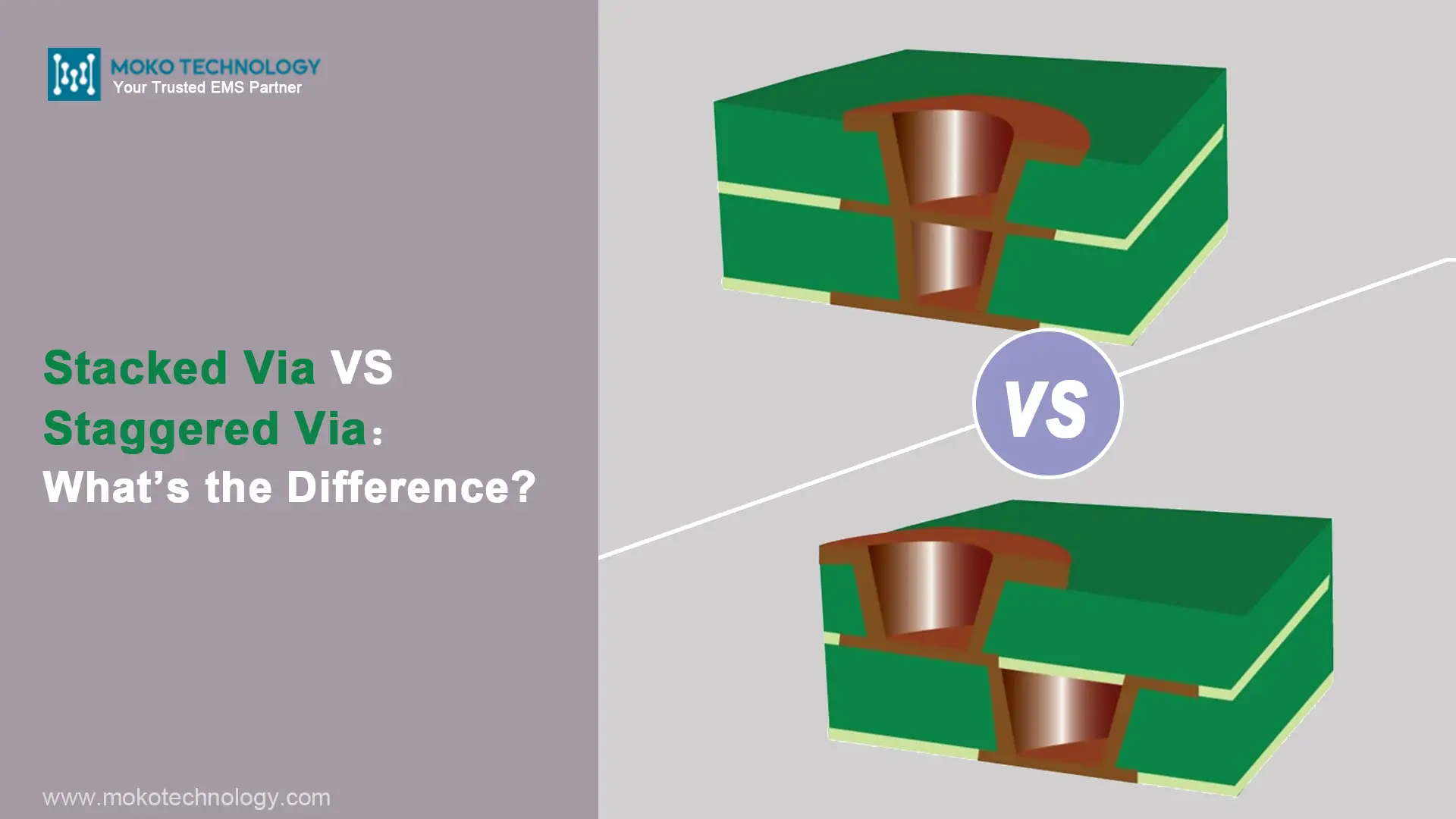
A common question when designing complex printed circuit boards for advanced electronics is whether to use stacked or staggered vias to route connections between layers. Vias act as conductive pathways through the interior layers of multilayer circuit boards. Understanding the key differences between vertically stacking vias atop one another versus horizontally offsetting them enables choosing the right approach for a given application and board complexity. This blog introduces these two types of vias and compares them from different aspects to help you make an informed choice between the two when designing your PCB.
Stacked Via in PCB
PCB stacked via is a type of PCB via used in printed circuit boards to make electrical connections between non-adjacent layers, providing an optimized vertical routing solution in one compact structure. Constructed by drilling a single hole through two or more adjacent PCB layers and then plating the hole walls to connect the vias electrically, stacked vias enable shortcuts between distant layers without having to route horizontally across the layers in between. With their ability to streamline trace routing paths between multiple board layers, stacked vias help reduce circuit congestion and clutter compared to alternate connection methods. Offering condensed footprints plus multi-layer reach, stacked vias have become indispensable for complex, dense PCBs needing to drive signals seamlessly between many layers. Integrating efficient design with connectivity, PCB stacked vias deliver versatile, space-saving layer-to-layer transitions.
Staggered Via in PCB
Staggered vias are a type of via used in high-density interconnect (HDI) printed circuit boards to make layer-to-layer connections without having vias directly lining up. Constructed by offsetting the positions of vias on adjacent layers and then drilling holes at an angle, staggered vias prevent adjacently stacked vias from physically contacting. This angular, indirect alignment removes the need for filling copper around typically stacked plated-through vias, streamlining fabrication. Acting as blind and buried connections between inner and outer layers, staggered vias enable shorter and more efficient routing pathways not possible with vertically adjoining via placements. Careful attention during design is necessary when determining appropriate stagger spacing between vias to meet minimum separation clearances. While physically separating vias requires more complex layouts and drilling operations, staggered vias eliminate superfluous metal fill requirements and provide unique routing capabilities. Ultimately, the interconnected functionality of staggered vias translates to denser, higher performing printed circuit boards.
What Is the Difference between Stacked Via and Staggered Via?
- Space Efficiency
Stacked vias: By lining up the vias in a vertical column through all layers, stacked vias consume the minimum necessary footprint area since they overlap perfectly across layers. This makes them ideal when space is constrained. The vertical condensing also allows for bringing connections closer together.
Staggered vias: Since staggered vias intentionally shift position on alternating layers, additional clearance has to be designed around each via on every layer to maintain spacing. This consumes more total board area compared to stacked vias. But the shifting does eliminate vertical alignment which helps with crosstalk.
- Crosstalk Issues
Stacked vias: With vertically stacked vias, the risk of electrical crosstalk interfering with high-speed signals is increased along that axis. Noise can propagate easier across layers when vias directly line up. Additional spacing helps control crosstalk.
Staggered vias: By offsetting vias between layers, staggered vias avoid continuous vertical alignment which greatly reduces the likelihood of crosstalk issues by eliminating the vertical coupling path. Noise is isolated between layers.
- Filling Requirement
Stacked vias: Because electrical connectivity through all layers is critical with stacked vias, they usually require conductive hole filling between layers, typically with electroplated copper. This ensures robust, reliable electrical contact along the entire depth of the vertical via column even if the via hole walls have inconsistencies.
Staggered vias: For staggered vias, conductive hole filling between layers is generally only needed for vias that connect to the outermost PCB layers. Intermediate connections can remain air-filled so long as enough overlap is designed between adjacent vias to account for layer-to-layer misalignment.
- Via Arrangement
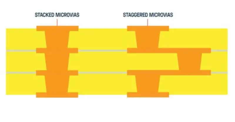
Stacked vias: Stacked vias are vias that directly overlap and are interconnected through multiple layers of a printed circuit board. They form a vertical column going through different layers, essentially stacking one via right on top of the other along the same x-y axis coordinate location on different board layers. This minimizes the total board area consumed.
Staggered Vias: Staggered vias describe an intentional offset of the via placement on sequential PCB layers. Rather than being stacked vertically, staggered vias shift the via position slightly on alternating layers to prevent the drilled holes from being directly lined up. There is an intentional offset designed into the board layout.

- Economic Influences
Stacked Vias: Challenging precision mandates with stacked vias leads directly to heightened rejection rates once fabrication faults occur. Scrap loss from low yield drives up rework costs noticeably.
Staggered Vias: Fabrication processes accommodate looser staggered via tolerances easier with less scrap loss thereby improving manufacturing yield for cost savings. This makes scaling to higher volumes economical.
Closing Words
In summary, stacked vias and staggered vias both offer unique strengths that serve specific needs during multilayer PCB design. Stacked vias maximize space by efficiently lining up paths between layers. Meanwhile, staggered vias enhance electrical isolation and simplify fabrication. When designing boards, electrical engineers weigh size constraints, manufacturing methods, timelines, and performance needs to determine ideal via placement strategies. By leveraging a mix of stacked and staggered vias when appropriate rather than rigidly sticking to one approach, engineers can enhance layout optimization and ensure production yield for innovative yet reliable PCB solutions. Evaluating tradeoffs allows embracing the complementary advantages of both vertically connecting and horizontally offsetting vias based on circuit requirements.
