Mastering Selective Soldering: A Comprehensive Guide


Selective soldering plays a crucial role in electronic manufacturing, holding significant sway over the excellence and trustworthiness of printed circuit board (PCB) assemblies. With the ongoing trend of products becoming more intricate and compact, gaining a firm grip on the art of selective soldering stands as a pivotal factor in generating resilient, high-output solder connections.
Delving into the depths of this blog, you’ll uncover a thorough initiation into the realm of selective soldering. Whether you’re setting foot into the realm of selective soldering for the first time or actively seeking to refine an already established procedure, this comprehensive guide stands ready to furnish you with the wisdom necessary for accomplishing successful selective soldering implementations.
What Is Selective Soldering?
To begin, selective soldering is a PCB soldering technique where solder is only applied to the areas that require a solder joint. Unlike wave soldering where the entire underside of the PCB makes contact with a wave of molten solder, selective soldering uses a miniaturized solder wave or fountain to target individual solder pads. The mini solder wave lets us be precise about which parts get soldered and avoids issues that can come up when everything gets dunked in solder all at once. So, selective soldering works well for PCBs with lots of components that are very close to each other. As electronic products are designed to be smaller and more precise, this soldering technique is more widely used.
Selective soldering systems utilize pumps to control solder flow, miniaturized solder nozzles, specialized tooling and automation, and thermal management systems. This enables the creation of an optimized, highly controlled soldering process capable of producing reliable solder joints on even the most complex boards.
Understanding the Selective Soldering Process


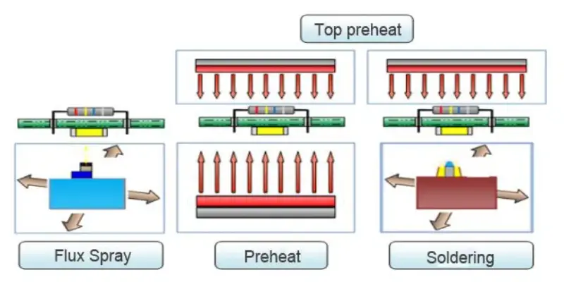
- Flux Application: Establishing the Foundation
The first step is applying flux – a special chemical that preps everything for soldering. Don’t let the name “flux” fool you, this stuff is crucial! It cleans the components and solder pads, removing any dirt, oil, or oxidation that could get in the way of the solder sticking. Flux makes sure the surfaces are super clean so the liquid solder can spread smoothly and adhere nicely. You can think of it as giving everything a careful cleaning to create the ideal, pristine environment for soldering.
- Preheating: Gradual Temperature Elevation
The next step after applying flux is preheating. This means slowly raising the temperature of the circuit board before we actually solder anything. We keep the preheat temp a bit below the melting point of the solder. Gradually warming up the board like this helps prevent thermal shock – big, sudden temperature spikes that could damage the sensitive components. It’s a gentle way to get the board acclimated and ready for soldering, like helping your body adjust before jumping into a hot tub. Preheating takes things slow so the components aren’t startled by rapid temperature changes once the soldering starts.
- Soldering: Precision Redefined
In this step, we use mini solder waves or nozzles to deposit solder right where we want it, right on the exact solder pads on the board. These tools let us orchestrate the soldering so precisely, putting that liquid solder in the perfect spot every time. Then we apply heat, and the solder melts and flows, forming connections with the components. In the end, we get reliable and structurally sound solder joints.
- Cooling Down: A Delicate Conclusion
After soldering is complete, the circuit board must be cooled gradually back to room temperature. A controlled, systematic cooling process is vital to avoid subjecting components to thermal shock from sudden temperature drops. Rapid cooling could create damaging stresses and strains from differential expansion and contraction. Like a glass dish cracking from hot water poured too quickly, rapid cooling can overstress fragile electronics. By cooling the board slowly, we allow time for the components to stabilize and acclimate as they transition from the high soldering temperature. This precautionary gradual cooling protects the integrity of the soldering work.
In essence, the selective soldering process weaves together the symphony of flux, calibrated heat, precision soldering, and controlled cooling to craft solder joints.
Advantages and Disadvantages of Selective Soldering
It’s wise to fully understand both the major advantages this process provides as well as any possible drawbacks or restrictions to keep in mind.
Advantages
Selective soldering blows other soldering methods out of the water and has become so essential for advanced PCB manufacturing. The super precise, controlled soldering lets you nail the sweet spot every time, only putting solder exactly where you need it. This minimizes defects and reduces stress on the components from heat. Even tricky stuff like soldering BGAs is no sweat. The closed-loop feedback also lets you dial in the ideal settings and optimize as you go. On top of all that, you get faster throughput, easier inspection, and the ability to solder mixed component types on one board. This soldering method brings a ton of upside that takes circuit board fabrication to the next level.
Disadvantages
However, selective soldering does come with some disadvantages to factor in as well. The selective soldering machine required has notably higher costs compared to simpler soldering methods. Programming and setting up the soldering process can be more complex and time-consuming. There are also potential limitations in terms of board size and flux residue buildup. Carefully weighing these pros and cons is important when deciding if selective soldering is the right choice for a particular manufacturing application. With proper planning and optimization, the advantages often make selective soldering the best process option for small, complex electronics requiring reliable and efficient soldering.
Selective vs. Wave Soldering
Comparison of Selective and Wave Soldering Processes
Selective and wave soldering represent two distinct soldering methodologies in electronics manufacturing, each with their respective strengths and applications.
Wave soldering involves conveying the printed circuit board across a standing wave of molten solder. This enables simultaneous soldering of multiple joints, making it well-suited for high-volume production scenarios. However, the generalized nature of wave soldering lacks precision, rendering it unsuitable for populated boards with sensitive components.
Conversely, selective soldering excels in applications where soldering accuracy and joint quality are of paramount importance. With its precise, focused deposition of solder, this soldering method is ideal for intricate PCBs containing both surface-mount and through-hole components. Although it may not achieve the throughput of wave soldering, its capacity to produce reliable, high-quality solder joints makes it the preferred method for specialized applications.
Furthermore, we offer a blog that compares wave soldering and reflow soldering. You can read it for reference: “A Comparison Between Wave Soldering and Reflow Soldering”.
When to Choose Selective Soldering
PCB Complexity: Selective soldering is ideal for complex PCBs with high component density and tight spaces.
PCB Component Types: When your PCB includes a mix of through-hole and surface-mount components, selective soldering is advantageous.
Quality Requirements: If your end product demands impeccable solder joint quality and reduced defects, selective soldering is a superior choice.
Avoiding Thermal Damage: Sensitive components that can’t withstand the heat of wave soldering benefit from the precision of selective soldering.
Best Practices for Successful Selective Soldering
Here are some key best practices for successful selective soldering explained in a bullet point list format:
- Optimize soldering recipes/programs for each board design – Account for differences in thermal mass and soldering requirements of each board. Use thermocouples and probes for real-time process control.
- Precise board alignment – Use solderable fiducials and proper tooling pins for accurate and repeatable board alignment. This is critical for precision soldering.
- Cleanliness – Keep solder nozzles, pots, and tools clean and debris-free through regular maintenance. This prevents defects.
- High-quality materials – Use proven no-clean solder paste and flux designed specifically for soldering processes. Don’t compromise here.
- Board layout – Allow enough clearance around solder joints to prevent bridging defects. Optimize layouts for soldering.
- Match process parameters – Tailor heaters, conveyor speed, etc. to match the thermal needs of each board design. This reduces stress.
- Inerting – Use nitrogen to prevent oxidation and enhance solder wetting. Oxygen-free environment improves quality.
- Monitoring and maintenance – Regularly inspect, monitor key metrics, and maintain the system to keep the process in control over time.
- Following these and other best practices tailored to each manufacturing environment allows companies to achieve reliable, high-quality soldering with maximum uptime.
Bottom Line
To recap, selective soldering is a super precise soldering method that nails those tiny, intricate circuit boards. Using the tips from this blog, electronics makers can establish a strong selective soldering process. This will majorly boost the quality, speed, and amount of boards pumped out. So in short, this soldering technique brings the skill to handle the fiddly stuff. Set it up right, and you’ll be cranking out pristine boards faster than ever.
Recent Posts
Impedance Matching: A Critical Factor in High-Speed PCB Design
Impedance matching has become a cornerstone of the signal integrity in the realm of high speed PCB…
How to Clean a Circuit Board Safely and Effectively?
It is important to learn how to clean a circuit board properly if you’re working…
Counterbore vs Countersink: Which to Choose for Your PCB?
When designing PCBs, selecting the appropriate type of holes for fasteners is crucial. And much…
PCB Copper Foil: Types, Properties & How to Choose
PCB copper foil is one of the most critical materials in the printed circuit board…
MOKO Technology Launches Vietnam Manufacturing Base in February 2025
Shenzhen, China - February 11, 2025 - MOKO Technology, a leading global electronics manufacturing service…
PCB Solder Mask: What It Is and Why Every Circuit Board Needs It?
While most people focus on the components and copper traces that make up PCBs, there's…


