In the world of printed circuit board design and manufacturing, precision and accuracy are paramount. One of the most crucial tools that ensures this accuracy is the PCB netlist. Whether you are an experienced engineer or a beginner in PCB design, knowing the netlist is always important. This comprehensive guide will explore what PCB netlists are, their various types, and their critical role in ensuring successful PCB production.
What Is A PCB Netlist File?
A PCB netlist is a text file that documents all electrical connections on a printed circuit board. В его ядре, it represents a collection of “nets” – electrical connections between two or more components such as resistors, конденсаторы, and other electronic parts on the board. This type of netlist, often referred to as a Schematic Netlist, includes the following key elements:
- A comprehensive parts list with unique designators
- Pin numbers and connection points for each component
- Contextual keywords and reference information
- Specifications and properties of component
The most important reason for a Schematic Netlist is to make sure that all of the electrical connections are right and there are no missing connection between components.

The Role of the Netlist in PCB Design
PCB netlists are fundamental to circuit board development, serving 3 critical roles as listed below:
- Capturing Potential Issues
Capturing potential problems before production gets started is one of the most critical functions of the netlist. The netlist gives engineers a clear list of connections that, если не правильно сделано, could cause failures during the testing phase. Например, if you have a missing or inappropriate connection in the netlist, if the PCB is fabricated and tested, this can cause considerable difficulties.
- Generating a Reference Netlist
Then during the Процесс изготовления печатной платы, once we load in the Файлы Гербера, the CAM (Computer Aided Manufacturing) program takes the Gerber data and the drilling data to create a reference netlist. A comparison is made of this reference netlist with the IPC-356 netlist to see where they differ. Comparing these lists gives manufacturers a heads up to verify that the design truly communicates an accurate depiction of an intended electrical connection, thus substantially cutting the risk of errors.
- Design Reuse
Design reuse is facilitated through the netlist, both because previously designed circuits or components can be easily used in the new project without introducing errors, and because they can be easily reused elsewhere. When you reuse a design, it is what makes up the netlist — all the electrical connections, all the component relations, so you keep the integrity of the original design.
How to Generate a Schematic Netlist?

Generating a schematic netlist involves the following key steps:
- Schematic Capture: Using schematic capture software to create the circuit design, where components are placed and connected with each other as per the circuit requirement.
- Проверка электрических правил (ЭРК): The schematic is ran through an Electrical Rules Checking (ЭРК) before actually net listing, to ensure that the design complies to a set of predefined rules and to detect potential errors or any violated rules.
- Netlist Generation: After the ERC, the schematic capture software will create a netlist file that normally are compatible with the PCB layout design software.
- Netlist Validation: After the netlist is generated, it needs to be verified against the original schematic design to ensure accuracy and completeness. This process can be done manually and automatically.
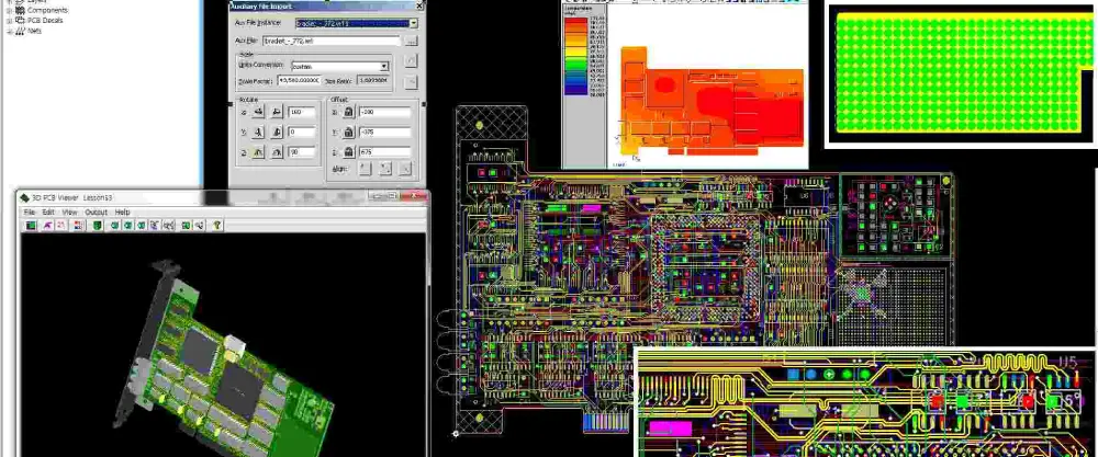
- Importing the Netlist: The netlist is validated and the netlist is imported into the PCB design software. Using this information, software will generate the preliminary layout of the PCB, and place component footprints and electrical connections.
- Проверка правил проектирования (ДРК): Once the PCB layout has been created, then we perform a Design Rule Check (ДРК). This steps makes sure that the design obeys some pre-defined rules, that it is manufacturable and conforms to industry standards.
The Importance of the PCB Netlist in Electrical Testing
After the PCB is manufactured, the netlist is still crucial in the electrical testing phase. To verify electrical continuity across the PCB, netlist based testing methods range from hard test fixtures to flying probe techniques. Поступая таким образом, all the endpoints will be correctly detected and can be verified thoroughly on the circuit’s functionality. Кроме того, PCB netlist can be used to compare expected and actual connections to make sure the circuit acts the way it should. With the netlist, engineers can quickly find and fix just about any issue and overall improve the quality of the PCB.
What Is the Difference between Schematic And Netlist?
Both schematic and netlist are constituent parts of the PCB design process, but they add different value and represent the design differently:
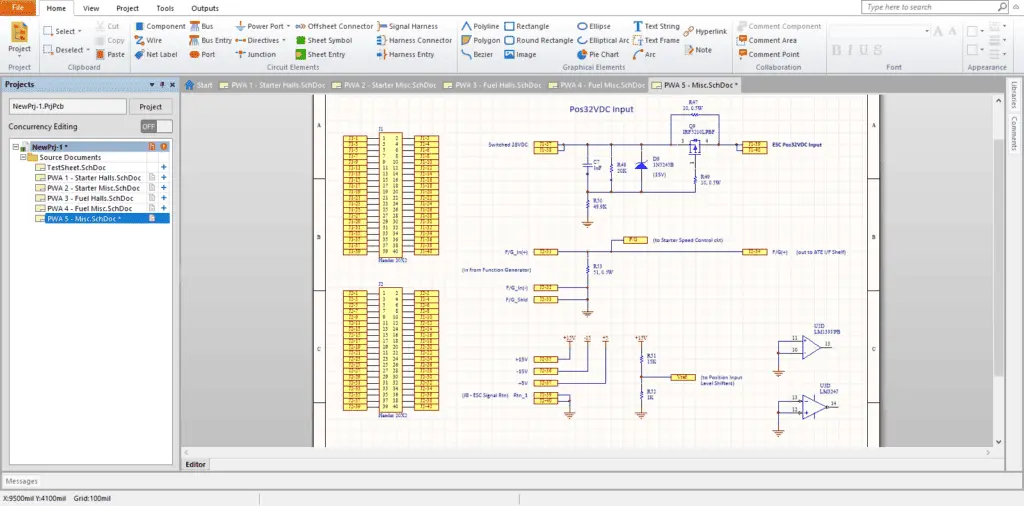
Schematic: The electrical schematic is a graphical analogy to the electrical circuit. It shows how resistors, конденсаторы, IC’s, etc are connected with wires or nets and it shows all components with their values. The schematic shows an engineer the design and plans of the circuit, details about how the connection of the components works and exactly how the circuit is supposed to behave physically. It also includes component values, part numbers and pin configurations.
Netlist: Иначе, the netlist is a text or data file containing a list of electrical connections (the nets) between the components of the schematic. It has a list of all the components that are present and what their pins are and how they are connected, but doesn’t contain any graphical or physical representations. Mainly for PCB layout software to place components and route outlines, the netlist is the primary input. It does the conversion of the electrical connections from an schematic to the PCB design such that they are translated accurately.
Other Types of Netlist And Their Applications
The IPC-D-356 Netlist
IPCD-356 Netlist is created for PCB testing and verification. Unlike simpler netlist formats, it retains comprehensive information about test points, board layer stackup, and component location, and net names in a uniform format. This is very valuable in automated testing equipment such as In-Circuit Testers (ИКТ) and Flying Probe machines, allowing manufacturers to fully test a printed circuit board.
Gerber Netlist File
A Gerber Netlist File (normally with a .net extension) describes the electrical interconnections and components of a circuit board as a text based file format used in printed circuit board manufacturing. It provides information as to which of the component pins should be connected together electrically so that manufacturers can verify that the electrical design of the PCB is consistent with the physical layout of the PCB. It is useful as a quality control tool when used in conjunction with Gerber files, the manufacturers can perform electrical testing by comparing the actual board connections to the netlist to ensure all connections are made and no unintended shorts or open circuits.
Заключение
Electronic design and manufacturing rely heavily on PCB netlist as one of the fundamental tools. Netlists aid in ensuring the accuracy and functionality of printed circuit boards, from initial design verification to final testing. Proper netlist verification understanding and implementation can result in better manufacturing results and greatly reduce errors. In MOKO Technology, we believe in the importance of doing a thorough netlist verification process before delivering any circuit board to customers, as we strive to make all circuit boards we produce to be of the highest quality and reliability.


