Пайка SMD — это процесс пайки электронных компонентов поверхностного монтажа к печатным платам.. Поскольку электронные устройства и печатные платы становятся все меньше, использование SMD-компоненты резко вырос в схемотехнике. Крошечный размер компонентов SMD обеспечивает гораздо большую плотность компонентов на печатных платах и позволяет миниатюризировать современную электронику.. тем не мение, их небольшой размер также создает некоторые уникальные проблемы при сборке и пайке. В этом руководстве, мы рассмотрим ключевые инструменты & материалы, the step-by-step process for properly soldering SMD components and master SMD soldering rework.
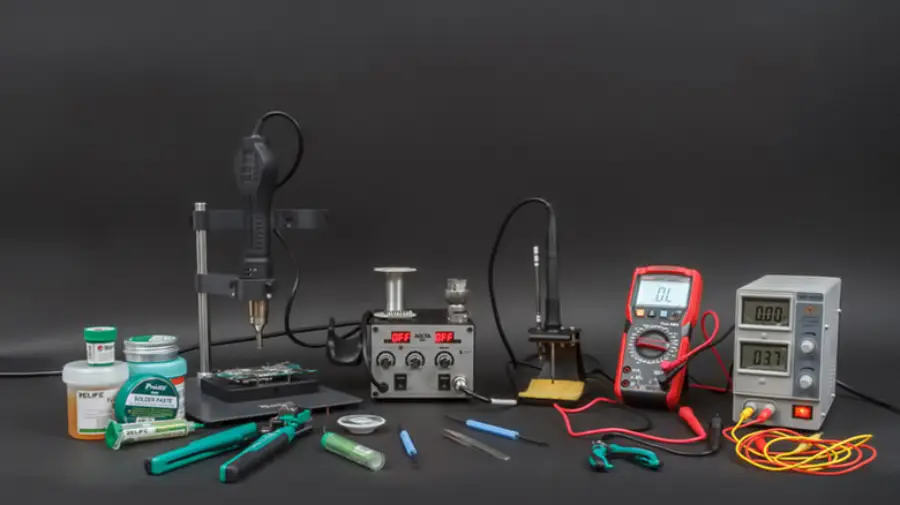
Существенный Инструменты для пайки SMD & Материалы
Для пайки устройств поверхностного монтажа требуются специальные инструменты для работы с крошечными компонентами и выполнения точных паяных соединений.. Вот некоторые из предметов первой необходимости, которые вам понадобятся:
Паяльник — Паяльник с тонким жалом мощностью 15–30 Вт идеально подходит для работы SMD.. Можно использовать наконечники размером до 0,5 мм.. Функции контроля температуры помогают избежать перегрева..
Hot Air Soldering Gun – Use hot air to melt solder or solder paste, equipped with different gun tips.
Флюс – Usually rosin solution or flux paste. Pen-type or needle-type applicators allow for better control of the amount used.
Cleaning Agent – PCB cleaner or isopropyl alcohol, usually combined with a brush or cotton swabs, is used to remove residual flux.
Solder Paste– Solder paste consists of a mixture of powdered solder alloy and flux cream. Это позволяет точно наносить припой на площадки SMD перед установкой компонентов..
Микроскоп. Стереомикроскоп или увеличительное стекло незаменимы для проверки небольших паяных соединений и расположения компонентов.. Обычно используется микроскоп с увеличением от 20 до 40 раз..
Пинцеты. Пинцеты с тонкими кончиками позволяют точно манипулировать и размещать компоненты SMD размером до 0201 или же 01005 размеры (0.25мм х 0,125 мм). Предпочтителен антистатический пинцет..
Руки помощи при пайке – инструменты для рук с увеличительными линзами позволяют без помощи рук позиционировать печатные платы под микроскопом во время пайки..
Stencil – Трафареты для печатных плат представляют собой тонкие металлические листы, вырезанные лазером, с рисунком отверстий, соответствующим расположению паяной площадки на печатной плате.. Для нанесения паяльной пасты, трафарет выравнивается по печатной плате, и паста распределяется по контактным площадкам через отверстия трафарета. Использование трафарета позволяет точно и эффективно наносить паяльную пасту перед размещением SMD-компонентов..
Приспособления — приспособления помогают расположить платы под углом, что улучшает видимость и доступ к паяным соединениям под компонентами во время ручной пайки..
Инструменты для присоски/демонтажа припоя. Специализированные вакуумные инструменты используются для удаления или доработки паяных соединений и компонентов для демонтажа припоя при ремонтных работах..
How to Do SMD Soldering: A Professional Step-by-step Guide
Подготовьте печатную плату, тщательно очистив ее от мусора и окисления, которые могут присутствовать.. You can then start SMD soldering with a soldering iron or a hot air soldering gun.
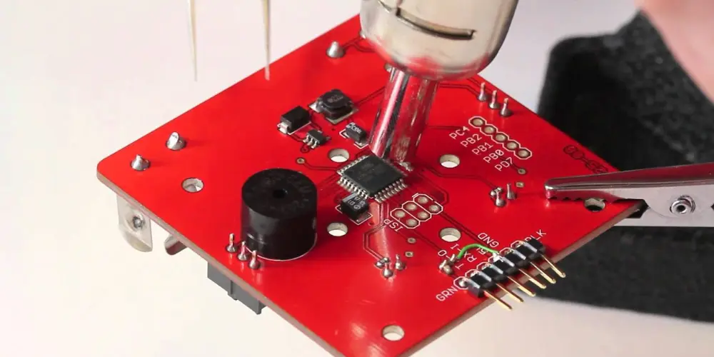
SMD пайка with Soldering Iron
Шаг 1: Применение флюса
Use a flux pen to evenly cover all SMD pads with flux. For leadless ceramic ICs, pre-tin pads with solder (work quickly at a moderate temperature to avoid over-melting).
Шаг 2: Размещение компонентов
Use anti-static tweezers to precisely place the chip on the Печатная плата колодки. Check thoroughly to ensure that each terminal is aligned with its respective pad.
Шаг 3: Corner Tack Soldering
Put a little solder on the soldering iron tip to solder the diagonal corners of the chip and hold it in place. Recheck alignment before the next step.
Шаг 4: Flux Reapplication
Use the flux pen again to apply a fresh layer of flux over the pins and pads, ensuring smooth solder flow and preventing oxidation.
Шаг 5: Drag Soldering with a Mini Wавеню Тip
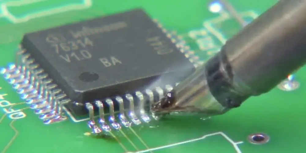
Use a mini wave tip to drag soldering, which has a solder reservoir at its head. Firstly load the reservoir with molten solder. Gently touch the outer ends of the pins and QFP pads with the tip. Slightly lift the tip by about 0.5 mm to allow molten solder to flow from the reservoir into the pad and pin area, forming a solder joint. На этом этапе, pay attention to the hand gestures. The axis of the soldering iron tip should form an angle of 30°to 45°with the edge to be soldered. Do not drag soldering too fast, and control it to drag through one soldering point in about 1 второй.
Шаг 6: Заключительная проверка & Очистка
Once soldering, thoroughly inspect each solder joint under a microscope to check for any shorts or poor soldering that require rework. For short circuits, apply flux and re-drag (Максимум 2 attempts per area). If the soldering is not done properly once, wait until it cools down before soldering again. (≤3 reworks total). While there are no defects, perform a clean process.
SMD пайка с участием Hot Аir Soldering гun
Шаг 1: Pre-Soldering Inspection
Inspect the PCB pads for adequate solder bumps. If the solder amount is insufficient, apply a small amount of solder on the pads with a soldering iron. If there is no solder bump, deposit solder paste on the pads using the PCB stencil.
Шаг 2: Применение флюса
Apply flux to both the component pins and the pads to improve adequate wetting during the reflow process.
Шаг 3: Размещение компонентов
Use tweezers to position the SMD component accurately on the PCB pads. Make sure the leads are properly aligned with the pads.
Шаг 4: Предварительный нагрев
Before soldering, use the hot air gun to gently preheat the area around the component. This prevents thermal shock and ensures even heating.
Шаг 5: Оплавление Процесс пайки
Apply hot air to the component evenly till the solder melts and reflows. For small SMD components, surface tension will help the component auto-align into the correct position. When working with QFP components, pay attention to pin alignment during heating. It’s recommended to solder one row of pins first, verify for alignment, and then solder the other rows.
Шаг 6: Заключительная проверка & Очистка
После завершения пайки, inspect for any potential defects. Clean the circuit board with isopropyl alcohol and a brush or cotton swabs to eliminate any residual flux.
Советы, которым следует следовать в процессе пайки
- Используйте самую низкую эффективную температуру паяльника, чтобы не повредить чувствительные компоненты..
- Содержите жало паяльника в чистоте между соединениями, чтобы обеспечить оптимальную передачу тепла к соединению..
- Apply just enough solder to form a proper fillet on each joint. Insufficient or excess solder can lead to unreliable connections.
- Следите за растеканием и смачиванием припоя и при необходимости повторно нанесите флюс или предварительно оловянные площадки..
- Не прикасайтесь к печатной плате и не ударяйте ее, пока все паяные соединения не остынут и не затвердеют..
- Visually inspect underneath components like BGAs and QFNs if possible.
- Брать ESD prevention steps like grounding wrist straps and mats.
- Работайте систематически от центра к краям или от мелких компонентов к более крупным..
- Сохраняйте площадки прохладными, избегая длительного нагревания в одном месте, чтобы предотвратить подъем площадки или повреждение печатной платы..
How to Do SMD Soldering Rework?
Пайка устройств поверхностного монтажа — это деликатный процесс, но необходимый навык для ремонт печатной платы и модификация. Хотя необходимо соблюдать большую осторожность, можно успешно отпаивать и заменять SMD-компоненты, не повреждая плату. We will then introduce how to do SMD soldering rework using a hot air soldering gun and a soldering iron.
Desoldering with a Soldering яron
Apply flux on the component pins and select an appropriate soldering iron tip with 200-400℃ temperature. Heat the pins to melt the solder and remove the components with tweezers. The operation is slightly different for various types of components. The following are the specific details.
Two-Terminal SMD Components – Begin by applying solder to one end and heating it using the soldering iron. While the solder is melting, quickly heat the other end. When both ends are molten, use tweezers to remove the component. You can use two soldering irons to heat both ends at the same time.
Двойной линейный пакет (ОКУНАТЬ) ИС – Apply flux to the pins, then pile solder along one row. Move the soldering iron along the row of pins to melt the solder. Insert tweezers between the IC and pads on the molten side and lift to separate the pins. Remove excess solder with a soldering iron or solder wick. Repeat the operation for the other side to remove the component thoroughly.
Четырехместный пакет с плоским экраном (QFP) ИС – Apply flux to the pins and solder wick. Place the solder wick over the row of pins and heat with a soldering iron. Insert a thin non-wettable steel shim between the pins and the pads to lift them. Repeat for all sides until the chip is off.
Desoldering with а Hot Air Gun
Apply flux on the component pins and hold the components with tweezers. Preheat the components around with a hot air gun, then blow on the components. Do not stay in one place and move the hot air gun head quickly to heat each pin. When the pin solder is melted, remove the components with tweezers. Ну наконец то, clean the pads for re-soldering.
What you should keep in mind:
-Perform the overall pre-heating, usually for 30 секунды.
-Choose the gun tip according to the shape of the component, using a tubular gun tip in general.
-Keep the gun tip perpendicular to the circuit board as much as possible and about 10 mm away from it.
-В целом, set the wind speed to 1-3 levels and heat to 5 levels.
Последние мысли
Пайка SMD поначалу может показаться сложной задачей из-за работы со смехотворно маленькими компонентами и соединениями.. Но с некоторой практикой, правильные инструменты, и следуя твердой технике, вы можете успешно паять компоненты практически любого размера. Компоненты для поверхностного монтажа становятся все меньше, а платы более плотно упакованы., Обучение навыкам пайки SMD становится обязательным для всех новичков в области печатных плат и любителей электроники..