Os dispositivos eletrônicos estão avançando rapidamente, eles exigem designs compactos e eficiência. Entre muitas escolhas que importam, Os pacotes QFN são uma escolha popular de todos os tempos. O que torna esse tipo de pacote tão popular? Você também deve usá-lo em seus projetos? Este guia apresenta uma visão clara e abrangente do assunto.
O que são pacotes QFN?
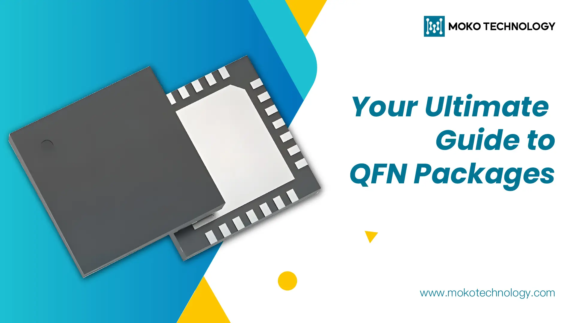
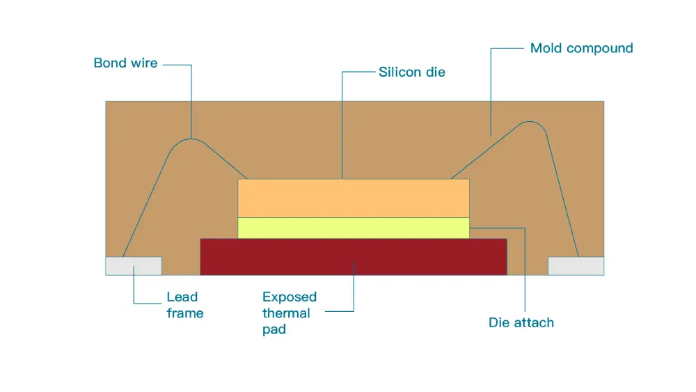
QFN significa Quad Flat No-leads. Pacotes QFN anexam matrizes de silício (o ASIC) para uma placa de circuito impresso (PCB). É implementado usando tecnologia de montagem em superfície. Como o nome sugere, este pacote não incluía os leads clássicos que existiam no passado. Em vez de ter leads habituais, Os pacotes quad flat sem chumbo possuem almofadas de borda com abertura almofada de solda sob. Esta estrutura pode melhorar o desempenho elétrico e térmico, e é por isso que os pacotes QFN são muito populares entre os usuários.
Um pacote QFN geralmente consiste nos seguintes componentes básicos:
Quadro principal: Esta parte é muito crítica para determinar o desempenho do IC. Basicamente serve como suporte para o pacote.
Matrizes simples ou múltiplas: Na verdade, esses são os chips de silício dentro do pacote e são montados na placa de circuito usando a técnica de montagem em superfície.
Obrigações de fio: Geralmente são feitos de cobre ou ouro. Esses fios formam as conexões necessárias entre a estrutura condutora e as matrizes.
Composto para Moldagem: Este material envolve e protege os componentes internos. Fornece isolamento elétrico, evita corrosão, e fortalece a durabilidade e confiabilidade do pacote.
Tipos de pacotes Quad Flat No-Lead
- QFN de cavidade aérea: Este tipo é caracterizado por uma tampa de plástico ou cerâmica, uma estrutura de chumbo de cobre, e um corpo moldado em plástico que não é selado. Este tipo é geralmente usado em sistemas de microondas que operam entre 20 para 25 GHz, onde uma cavidade de ar é necessária
- Pacote QFN de múltiplas linhas: Este tipo de projeto atende aos requisitos de um grande número de pinos usando múltiplas fileiras de pinos, igual a Tecnologia BGA mas muitas vezes é feito a um preço mais baixo.
- QFN com flancos molháveis: Este tipo de pacote quádruplo plano sem chumbo expôs flancos ou terminais de metal em todos os quatro lados do corpo do pacote. Todos esses flancos são projetados para serem molháveis por solda e desta forma, a solda terá a possibilidade de absorver e fazer uma forte conexão de solda entre o pacote e o PCB.
- Pacote Fc-QFN (Flip-Chip Quad Flat sem chumbo): Ele usa conexões flip chip em uma estrutura de cobre. E é menor que um pacote QFP normal e também melhora o desempenho elétrico devido ao fato de que o caminho elétrico é mais curto.
- Ligação de fio QFN: Em um pacote QFN wire bond, a matriz semicondutora é montada em um leadframe e, após, ligações de fio são usadas para conectar os terminais do pacote à matriz semicondutora. este, claro, ocupa uma área de embalagem menor em oposição ao normal Pacotes Quad Flat (QFPs) com fios expostos.
Tipo Punção QFN vs Tipo Serrado QFN
As embalagens QFN também podem ser divididas em dois tipos principais dependendo do processo de fabricação:
Tipo de punção QFN: Este estilo é produzido com uma cavidade de molde. Após o processo de moldagem, uma ferramenta especial é usada para retirar cada embalagem individual da matriz moldada.. Este método é muito produtivo para produção em massa e geralmente resulta em uma produção limpa., corte afiado.
Tipo serrado QFN: Por outro lado, QFNs do tipo serrado são produzidos através do processo de matriz de moldes. Isso envolve o processo de fazer uma grande folha de embalagens moldadas cortada em unidades individuais usando uma serra. A tecnologia é muito eficiente no gerenciamento de grandes volumes.
Vantagens e limitações dos pacotes QFN
Vantagens:
- Compacto e discreto, é ideal para aplicações com espaço limitado em dispositivos como smartphones, vestuário, e dispositivos IoT.
- Melhor dissipação térmica devido ao molde exposto que permite que a temperatura seja transferida de forma mais eficiente para a PCB.
- Maior eficiência térmica se traduz em melhor desempenho e confiabilidade.
- Bom para aplicações quando tamanho, peso, e consumo de energia são fatores muito críticos.
Limitações:
- Nenhum cabo externo facilita a inspeção visual ou o retrabalho das juntas de solda, que estão escondidos sob o corpo do pacote.
- Para espaçamento de pinos pequeno e um número maior de E/S, existe um risco maior de ponte de solda, e os processos precisam ser muito bem controlados para evitá-los.
- Não é muito ideal para alguns propósitos de alta confiabilidade.
QFP vs.. QFN: Qual é a diferença? Como escolher entre eles?
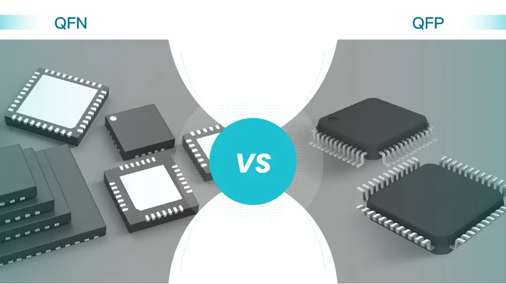
QFP e QFN são os dois pacotes de circuitos integrados mais comuns. Embora seus nomes difiram apenas por uma letra, o pacote QFP apresenta cabos em forma de asa de gaivota que se projetam do corpo do pacote. Isso é muito útil ao inspecionar ou retrabalhar, e ao mesmo tempo, é bastante compacto.
QFNs terão melhor dissipação térmica porque a almofada da matriz está exposta, e este tipo de design permite que mais calor seja transferido para o PCB. Contudo, QFNs são difíceis de inspecionar visualmente e retrabalhar devido ao fato de que as juntas de solda ficarão enterradas sob a embalagem.
Considere o espaço no quadro para o componente, a necessidade de desempenho térmico, e as capacidades do processo de fabricação. Se a necessidade é espaço e desempenho térmico, então QFNs podem ser a escolha, mas se facilidade de inspeção e facilidade de retrabalho é o que é necessário, então os QFPs podem ser a melhor alternativa.
Leitura adicional: Tipos de pacote IC: Como Escolher o Certo?
Aplicações de pacotes QFN
Os pacotes QFN são especialmente populares em setores onde economizar espaço e ter desempenho superior são de suma importância. QFNs são usados nos seguintes setores:
- Eletrônicos de consumo: O pacote quad flat sem chumbo é comumente usado em smartphones e tablet PCs com propósitos gerais de ocupar um espaço pequeno e ter excelente gerenciamento de calor.
- Sistemas Automotivos: O alto desempenho dos pacotes QFN faz dele um dispositivo usado em módulos vitais, como unidades de controle de motores.
- Aparelho de comunicação: QFNs encontram aplicação em dispositivos de rede de alta velocidade onde o processamento rápido de sinal é essencial.