É importante garantir que um projeto de PCB seja confiável porque qualquer erro de projeto, Não importa quão pequeno, pode retardar o processo de fabricação e montagem mais detalhada e, portanto, lead to higher expenses. As a beginner in PCB design, you will realize that more issues tend to arise compared to an experienced designer. Neste artigo, nós listamos o topo 10 common PCB design mistakes and give the corresponding solutions for newcomers to avoid these mistakes.
-
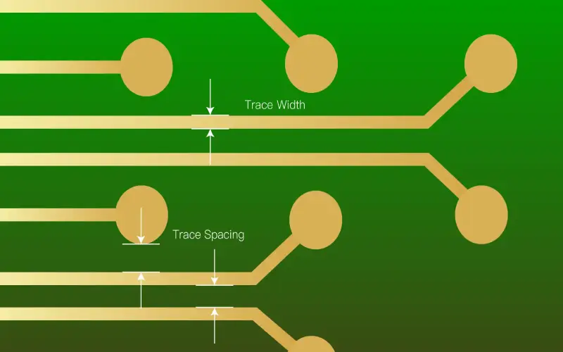
ImproperTrace Width
It’s tempting to use a uniform trace width throughout the board for simplicity, but this is not the best thing to do as different types of signals and power have varying requirements for trace widths. Por exemplo, traces that carry power have to be broader to dissipate heat with increased current flow without burning out. Por outro lado, high-impedance signals require narrow traces to minimize parasitic capacitance. Radio frequency signals are especially vulnerable and might require the exact value of trace widths to match characteristics impedance.
Leitura adicional: Largura do traço PCB: Por que é importante para o desempenho do seu conselho
-
Inadequate Trace Spacing
Manufacturers set minimum distance requirements for PCB production. Inexperienced designers, em particular, consider compliance with these minimums as the best option; Contudo, it leads to higher costs, lower yields, and more extensive trace-to-trace coupling. Less spacing results in increased crosstalk and noise, which results in poor signal quality. assim, it is suggested to keep enough space between traces, isso é, the distance between traces should be at least 3 times the distance between the signal layer and the next closest reference layer.
-
Excessive Trace Length
For traces that need to transfer high-speed signals, they should be designed to be short and straight. In the case of the excessive length, there is a risk of facing problems such as signal reflection, increased susceptibility to EMI, and increased costs. The trace can be considered a transmission line when the length of a trace is more than a tenth of the wavelength of the signal that crosses it. Nesse caso, besides the length, an impedance calculation (using one of the many specific tools, also free on the net) shall be done to verify impedance coupling and avoid losing signal power.
-
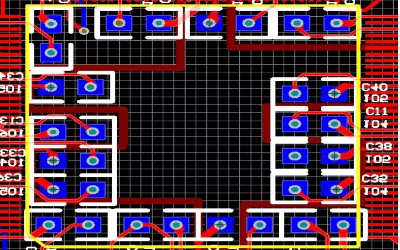
Wrong Position of Decoupling Capacitors
The PCB power supply lines must use desacoplamento de capacitores to provide all the board components with a stable power supply that is free from transients or oscillations. These capacitors are required to be always in parallel with the power supply input and should be located as close as they need to be to the pin of the component that requires power. The power line resulting from the power source must be well placed on the PCB so that it arrives at the decoupling capacitor before it goes to the pin that needs a stable voltage.
-
Place Parts Too Close to the Board’s Edge
In a PCB design, if you put the Almofada PCB too close to the edge, there may be a chance to damage the pad during assembly. A good design ensures that the pads are within the board’s boundaries. The standard tolerance of a PCB’s length and width is ±. 020 polegadas. If your board employs SMT in soldering components, then ensure you provide some extra space for your PCB manufacturers to grip the board perfectly during the SMT processo. Se não, your manufacturer will have to employ rails or fixtures to support the PCB – something that will increase your manufacturing costs.
-
Place SMT Pads Too Near to Each Other
SMT components have solder masks that are larger than the area of their pads. But individual solder masks should not intersect with each other. De outra forma, during the solder reflow, some of the parts may move toward the centre (and each other). You don’t need one large piece of copper and at the same time you do not want various parts to migrate to the center and collide with each other disrupting the manufacturing process and causing a variety of imperfections. To rectify such problems, there should be adequate space between the SMT pads.
-
Missing or Inadequate Vias
Vias are used for the interconnection of layers of a PCB and for heat dissipation. If vias are not properly employed, problems tend to arise such as poor signal quality and power distribution. It is recommended that designers should implement an appropriate number and size of vias for power and ground connection depending on the currents needed in the part and the frequency of signals. Thermal vias are relevant where there is a requirement of heat sinking in high power application areas.
-
Overusing Layers in the Design
There is no doubt that multi-layer PCBs offer many advantages such as increased routing space and enhanced Integridade do Sinal. Contudo, overusing layers when there is no necessary would only increase cost and make the fabrication process more complicated. Portanto, PCB designers must evaluate the circuit requirements carefully, considering better solutions like optimizing the component placement or using different routing strategies, instead of adding layers. An effective PCB design can achieve the same performance while also keep the cost within the budget.
-
Interferência eletromagnética (EMI)
The most common reason of electromagnetic interference is related to the poor design of printed circuit boards. Para minimize EMI in the PCB, it is suggested to group elements according to their functionality, such as the analog, digital, poder, low-frequency, alta frequência, or other circuits, etc. Ainda, it is appropriate to minimize on the, or preferably, do away with right angles on the traces and employ the use of metal containers and shielded cables that in turn allow for the absorption of interference.
-
Incorrect Antenna Layout
If PCB includes antennas for carrying out wireless communication, then laying down the circuit should be very carefully done in order to avoid committing mistakes. portanto, it is essential to match the impedance between the transceiver and the antenna to optimize the power transfer. Em geral, the cable line joining the transceiver to the antenna should ideally have an impedance of 50 Ω. For real and proper impedance adjustment, a Pi (LC) tuner filter, or any other matching circuit should be placed between the built-in antenna and the transceiver.
Leitura adicional: Como projetar uma antena PCB como um profissional?