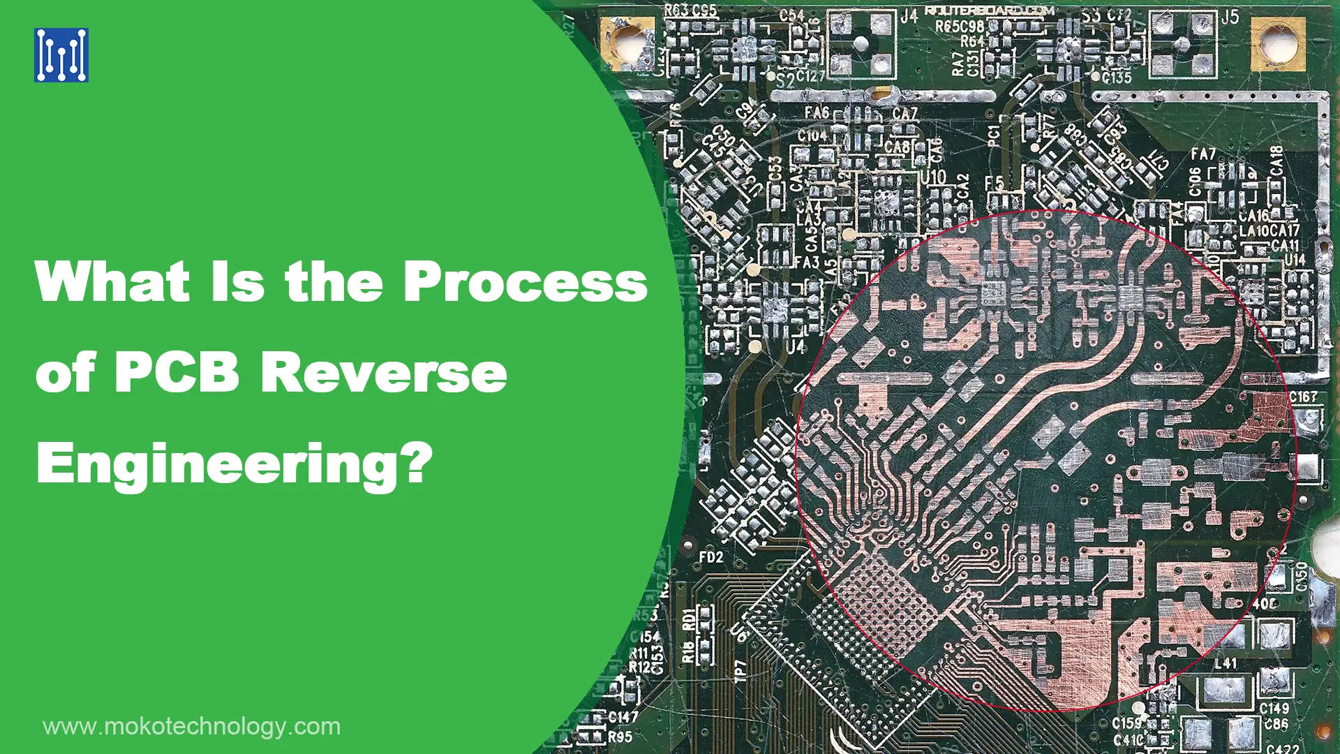
Inżynieria odwrotna PCB odnosi się do procesu analizy i zrozumienia projektu, układ, i funkcjonalność płytki drukowanej poprzez jej rozebranie, sprawdzając jego elementy, śledzenie jego połączeń, i tworzenie PCB schematyczny lub schemat układu bez dostępu do oryginalnych dokumentów projektowych lub planów. Inżynieria odwrotna PCB jest często wykonywana z różnych powodów, łącznie ze zrozumieniem, jak działa produkt konkurencji, odtworzenie wycofanej lub przestarzałej płytki drukowanej w celu naprawy lub modyfikacji, lub ocenę luk w zabezpieczeniach urządzenia. W tym poście na blogu, krok po kroku przedstawimy przegląd procesu inżynierii odwrotnej PCB, abyś mógł go lepiej zrozumieć. Zanurzmy się od razu.
Proces inżynierii odwrotnej PCB
Krok 1:
Zdobądź docelową płytkę PCB. Układ dokumentu poprzez fotografowanie i diagramy wszystkich pozycji komponentów, orientacje, i szczegóły na papierze, zwłaszcza diody, tranzystory, i luki w układach scalonych. Wyjaśnij, dobrze oświetlone zdjęcia całego zarządu w celach informacyjnych. W miarę jak płytki PCB stają się coraz bardziej złożone i zminiaturyzowane, śledzenie miedzi wizualnie pomaga w identyfikacji komponentów.
Krok 2:
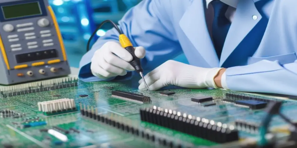
Usuń wszystkie elementy poprzez wylutowanie. Przed skanowaniem dokładnie wyczyść płytkę alkoholem izopropylowym, usuwając wszelkie zanieczyszczenia. Skanuj o godz 600+ rozdzielczość po delikatnym wypolerowaniu warstw miedzi, aby nadać im połysk. Zeskanuj oddzielnie górną i dolną warstwę w kolorze o wysokiej rozdzielczości, z tablicą całkowicie płaską względem powierzchni skanowania.
Krok 3:
Importuj skany do Photoshopa. Dostosuj poziomy, aż ślady miedzi będą dobrze widoczne i wyraźne od podłoża. Konwertuj dolną warstwę na czarno-białą i dokładnie sprawdź, aby mieć pewność, że podczas skanowania wszystkie przebiegi zostaną wyraźnie przechwycone bez rozłączeń. Zapisz zoptymalizowane warstwy jako pliki BMP o nazwach „TOP” i „BOTTOM”. Użyj oprogramowania, aby naprawić wszelkie defekty śladów widoczne na skanach.
Krok 4:
Otwórz pliki BMP w oprogramowaniu do projektowania PCB. Konwertuj do formatu natywnego. Użyj narzędzi do wyrównywania, aby nałożyć otwory podkładki, sposoby, i dokładne dopasowywanie punktów pomiędzy warstwami. Znaczące odchylenie wskazuje, że dla zapewnienia dokładności wymagane jest ponowne uruchomienie na wcześniejszym etapie.
Krok 5:
Zacznij od skanowania górnej warstwy. Odrysuj wszystkie widoczne elementy projektu, aby odtworzyć warstwę, dopasowanie rozmieszczenia komponentów do wcześniejszych zdjęć dokumentacyjnych. Trasuj połączenia po skanach, aby odtworzyć elektrycznie ślady miedzi. Usuń warstwę skanowania po zakończeniu śledzenia wektora. Powtórz proces dla dolnej warstwy skanowania, używanie narzędzi łączności do sprawdzania poprawności połączeń między warstwami. Dodaj wypełnione strefy dla wszelkich wewnętrznych płaszczyzn uziemienia/zasilania. Za ciasne płyty wielowarstwowe, włączyć tryby wyświetlania przezroczystości z prowadnicami wyrównania w celu dopasowania przelotek między warstwami.
Krok 6:
Wydrukować 1:1 folie górne i dolne, sitodrukowe. Ostrożnie nałóż je na docelową płytkę PCB, podświetlany, aby sprawdzić idealne dopasowanie wszystkich elementów do rzeczywistych płytek. Napraw wszelkie błędy poprzez dalsze modyfikacje śledzenia, aż do uzyskania pełnej walidacji.
Krok 7:
Dzięki formie i funkcji dokładnie uchwyconej i zweryfikowanej zgodności z oryginałem, Zakończono proces inżynierii odwrotnej płytek drukowanych. Dalsze testy obsadzonych płytek zbudowanych na podstawie zrekonstruowanych danych w celu porównania parzystości elektrycznej i sprawdzenia rzeczywistego powielania funkcjonalności.
Korzyści z inżynierii odwrotnej płytek drukowanych
Umożliwia regenerację przestarzałych płytek PCB – Inżynieria odwrotna może odtworzyć wycofane płytki drukowane, które nie są wspierane przez producenta oryginalnego sprzętu. Dzięki temu możliwa jest naprawa i dalsze użytkowanie sprzętu, który w przeciwnym razie byłby całkowicie bezużyteczny.
Ułatwia naprawę PCB – Poprzez zrozumienie projektu i komponentów PCB poprzez inżynierię odwrotną, Łatwiej będzie zdiagnozować usterki i wymienić komponenty naprawić uszkodzone deski.
Umożliwia niestandardowe modyfikacje i ulepszenia – Dzięki schematom i zrozumieniu projektu płytki drukowanej za pomocą inżynierii odwrotnej płytki drukowanej, inżynierowie mogą sugerować i wdrażać modyfikacje, takie jak dodawanie nowych funkcji lub zwiększanie wydajności.
Obniża koszty replikacji w przypadku małych serii produkcyjnych – Inżynieria odwrotna umożliwia tworzenie sklonowanych płytek PCB bez wysokich kosztów początkowej inżynierii i prototypowania, czyniąc produkcję na małą skalę bardziej przystępną cenowo.
Zapewnia wgląd w projektowanie interoperacyjności – Inżynieria odwrotna płytek drukowanych może analizować wewnętrzne działanie produktów konkurencji, co następnie wpływa na ulepszony projekt interoperacyjności.
Ułatwia postęp technologiczny – Szanując prawa własności intelektualnej, odpowiedzialna inżynieria odwrotna umożliwia dokładne badanie innowacyjnych projektów, rozpowszechnia know-how, i napędza dalszą kreatywność.
MOKO zapewnia niezawodną usługę inżynierii odwrotnej PCB
Technologia MOKO już prawie 20 wieloletnie doświadczenie w branży PCB, Oprócz Projektowanie PCB ., i montaż, świadczymy również usługi inżynierii odwrotnej. Z dogłębną analizą, odtwarzamy wycofane deski, klonuj istniejące, utracone z powodu starzenia się, lub zmodernizuj jednostki do nowoczesnych standardów.
Należy pamiętać, że inżynieria odwrotna może być legalna w pewnych okolicznościach, w niektórych przypadkach może to naruszać prawa własności intelektualnej lub naruszać ustalenia umowne. W związku z tym, niezwykle ważne jest, aby dokładnie ocenić i zrozumieć konsekwencje prawne związane z tym procesem. Nasz proces legalnie regeneruje płytkę PCB, przestrzegając granic własności intelektualnej. Przed rozpoczęciem pracy, dokładnie weryfikujemy projekty, aby zagwarantować brak naruszenia praw. Dzięki temu jesteśmy w stanie zapewnić w pełni funkcjonalne zamienniki, które można naprawić, replika, lub zwiększ wydajność swojej przestarzałej elektroniki. Skontaktuj się z naszym zespołem aby rozpocząć swój niestandardowy projekt już dziś.