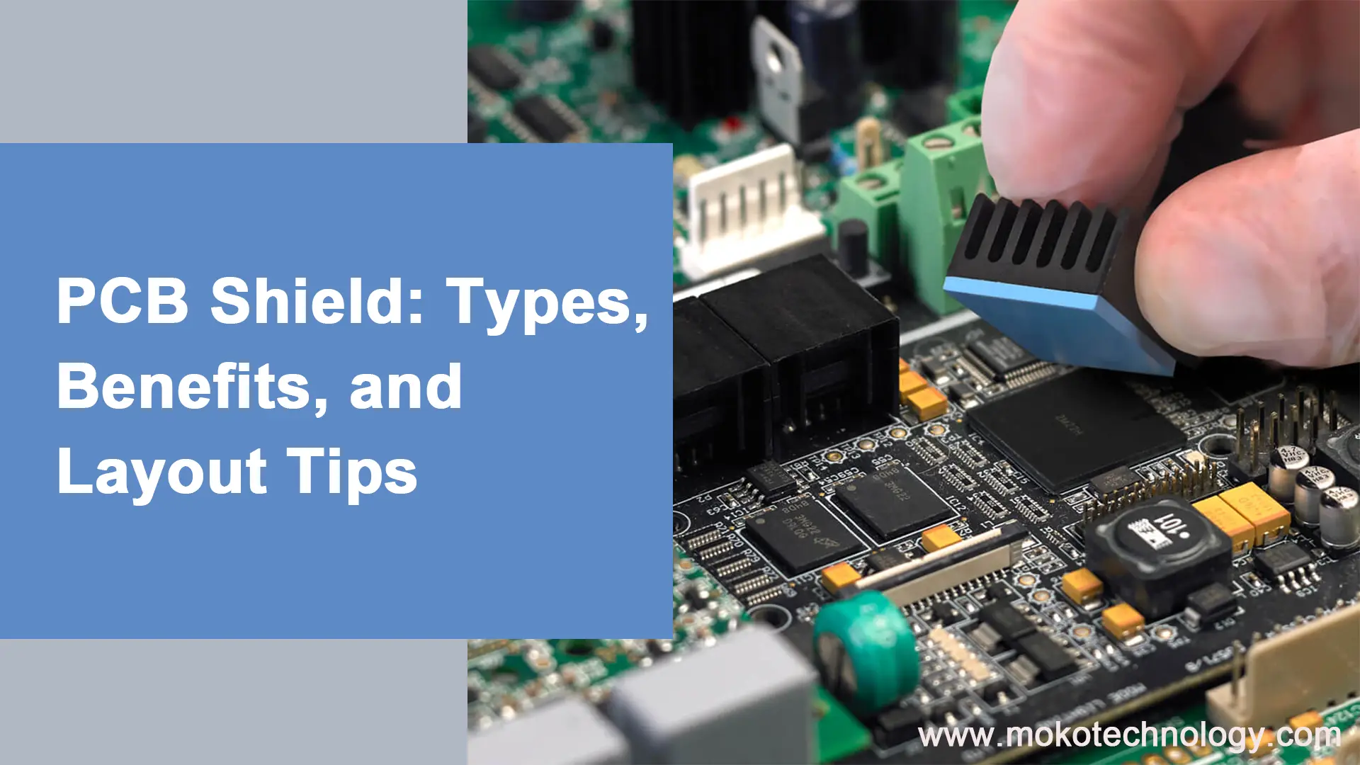
Płytka drukowana (PCB) Projektanci często borykają się z zakłóceniami elektromagnetycznymi podczas układania desek. Muszą wziąć pod uwagę kompatybilność elektromagnetyczną, aby spełnić specyfikacje systemu. Even small oversights in layout can spur electromagnetic complications, like short circuits or EMI/RFI noise. This is where a PCB shield comes in handy!
What Is a PCB Shield?
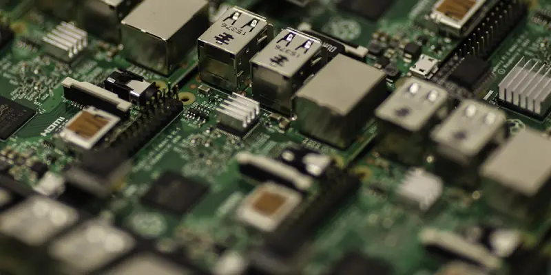
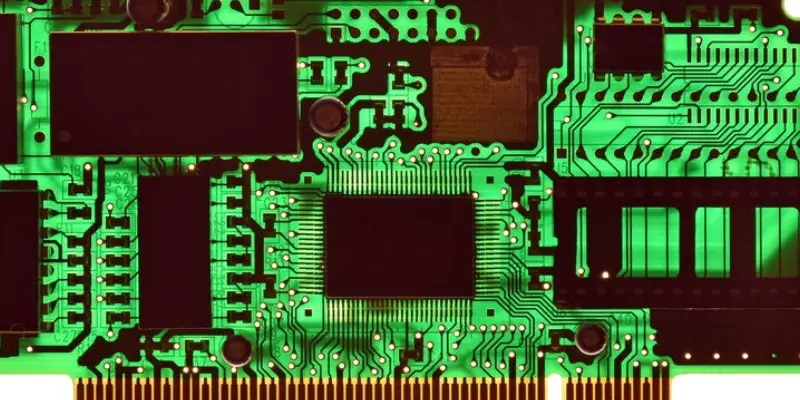
A PCB shield is an enclosure that surrounds your PCB to protect it and reduce electrical interference. It is usually made from a conductive metal material that acts as an electromagnetic shield. The most common materials used are aluminum, stal, and tin.
Shielding can prevent short circuits by protecting your PCB from contact with other components or surfaces. It also protects from dust and debris that could cause shorts. dodatkowo, it blocks electromagnetic interference (EMI) from radios, Motoryzacja, and other sources that can disrupt your sensitive circuitry.
Benefits of Using PCB Shield
Here are some of the key benefits of using a PCB shielding:
- Prevents short circuits – The shield prevents accidental shorts between lutować naramienniki or components on the PCB by isolating the electronics.
- Reduces EMI/RFI interference – Electromagnetic shielding blocks incoming and outgoing EMI/RFI noise that can interfere with your circuit operation.
- Protects from impacts – A rigid shield around the PCB helps protect from physical impacts, wibracja, and other mechanical stresses.
- Contains emissions – It blocks electromagnetic energy generated by your PCB from radiating out and interfering with nearby electronics.
- Improves safety – Shielding can reduce the risk of electric shocks by preventing contact with live components and circuitry.
- Allows prototyping – A shield lets you safely test and revise your PCB design more easily before creating a custom enclosure.
Types of PCB Shielding
Two prevalent shielding methods are radio frequency (RF) shielding and Arduino shielding:
-
PCB RF Shielding
RF shielding blocks electromagnetic fields, electrostatic charges, and radio waves. Common RF shielding solutions include metal cans, elastomer materials, ferrite beads and plates, conductive mesh, and isolated ground planes. These solutions act as Faraday cages, preventing external interference from disrupting sensitive components.
-
Arduino Shielding
Arduino shields are modular PCBs that attach to Arduino boards to add functionality. Na przykład, wireless, Ethernet, GSM, and prototyping shields expand Arduino capabilities. Shield pins connect the stackable boards while avoiding reserved pins used for I2C and SPI buses. With pre-built circuits and code libraries, Arduino shields enable quick implementation compared to custom designs.
Both RF and Arduino shielding have pros and cons. RF shields offer robust EMI protection but can be costly and complex to implement. Arduino shields are affordable and simple but provide less specialized shielding. Thoughtful shielding design is key to balancing protection, koszt, and complexity for a given application.
How does PCB Shield Work?
A PCB shield works by containing the electromagnetic fields from the PCB and blocking external EMI from other sources. The conductive enclosure forms a Faraday cage around the electronics, forcing EMI to flow along the outside of the shield. This prevents interference with components inside the shielded area.
Proper grounding of the shield also helps absorb radiated emissions and divert them to ground. Small openings are typically included to allow access to test points, wyświetlacze, and controls. Any gaps are minimized as much as possible.
6 Tips for Designing EMI Shielding in PCB Layouts
Mitigating electromagnetic interference in printed circuit board designs requires careful layout techniques. Following these 6 key strategies can help tame electromagnetic interference:
- Use a low-inductance ground plane.
Dedicate an entire layer on płyty wielowarstwowe as a ground plane. Maximize the ground plane area to reduce inductive loop area. This lowers the impedance of the current return path, reducing common mode noise and radiated emissions. Connect all signals directly to the ground plane using vias to avoid return path antennas.
- Shield sensitive components.
Use grounded conductive enclosures around components susceptible to interference. EM fields induce currents in the shield which cancel out the impinging fields through reflection and absorption. Choose appropriate shielding like cans, gaskets, or screens based on required attenuation.
- Control impedance with matched transmission lines.
Match trace impedance to source and load impedance using width/space ratio rules. This prevents reflections and resonances that cause ringing and EMI. Podążać kontrolowana impedancja design on high speed traces. Use impedance tuning stubs and termination resistors as needed.
- Bypass power rails with decoupling capacitors.
Place ceramic decoupling caps with low inductance right at each IC power pin. This provides a reservoir of charge to handle fast switching noise, keeping power rails clean. Use multiple capacitors with different values to target a wide frequency range.
- Segregate and filter board sections.
Partition board into analog, digital, high speed, etc and keep signals local. When signals must cross domains, filter using ferrites, common mode chokes and capacitors. This contains noise in each section.
- Organize component placement.
The group associated components together and orient uniformly. Place noisy digital circuits away from sensitive analog ones. Route traces efficiently to minimize length and crossing. Reduce antenna effects with periodic vias to ground.
Na wynos
Adding a proper PCB shield to your project can help prevent issues from short circuits, EMI/RFI noise, and static shocks. A careful shielding design is needed to fully contain unwanted electromagnetic interference. With robust shielding integrated into the PCB layout and enclosure, you can ensure the reliable operation of your electronics.