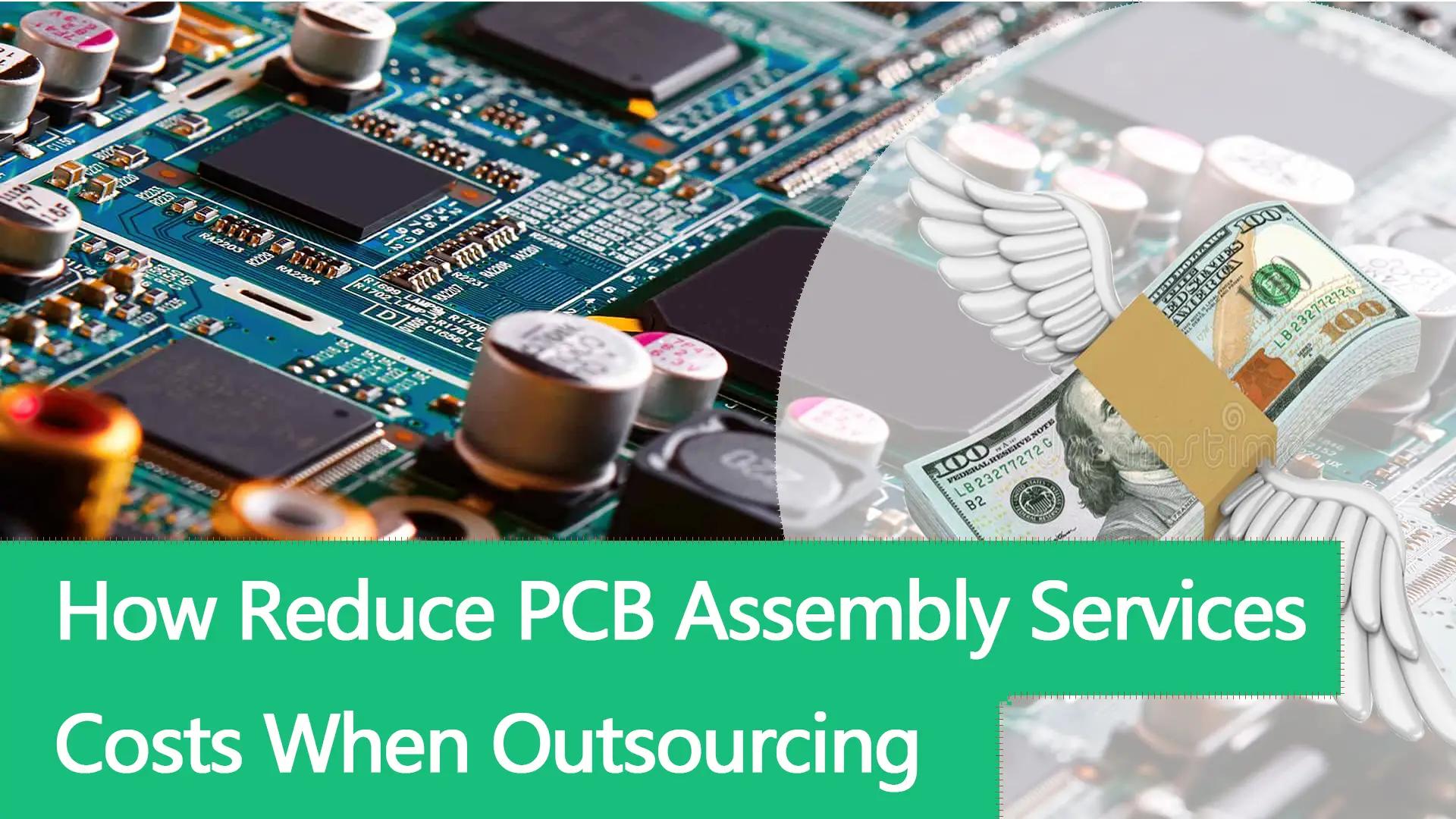
Jak obniżyć koszty usług montażu PCB podczas outsourcingu??
Coraz więcej firm decyduje się na outsourcing usług montażu PCB, oraz w procesie outsourcingu, ludzie często najbardziej martwią się o to, jak obniżyć koszty montażu PCB
Coraz więcej firm decyduje się na outsourcing usług montażu PCB, oraz w procesie outsourcingu, ludzie często najbardziej martwią się o to, jak obniżyć koszty montażu PCB
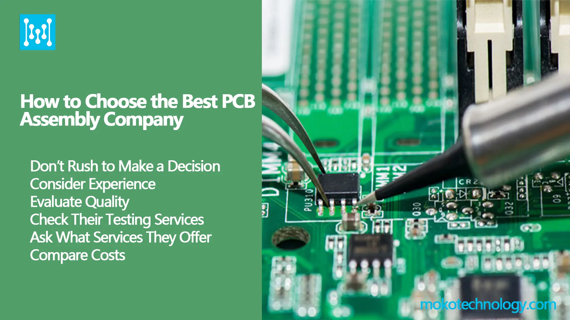
Montaż PCB nie jest łatwym zadaniem, które należy wykonać z doświadczeniem i starannością, aby upewnić się, że Twoje płytki działają zgodnie z projektem. W związku z tym, wiele firm, którym brakuje ekspertów
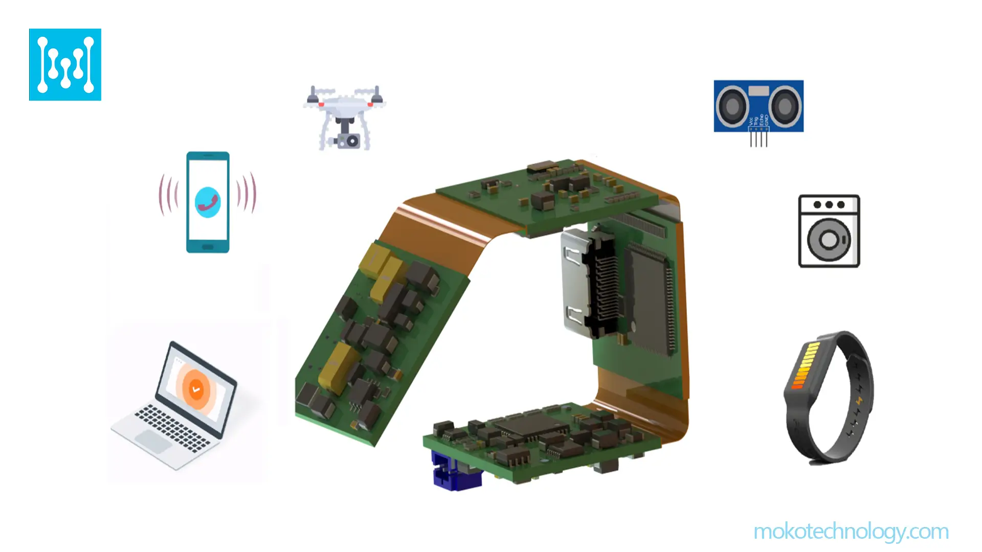
Montaż PCB SMT stał się najpopularniejszą technologią montażu PCB od lat 80-tych, i jest obecnie szeroko stosowany w branżach takich jak elektronika użytkowa, opieka zdrowotna, elektronika samochodowa, i telekomunikacja.
Rynek elektroniki użytkowej jest ogromny, Szacuje się, że konsumenci na całym świecie wydadzą około 505 miliardów USA. dolarów w 2022 na elektronice. Wraz ze stale rosnącym
Samochodowe płytki PCB są szeroko stosowane w różnych układach elektronicznych w samochodach, od ADAS i oświetlenia pojazdu po elementy informacyjno-rozrywkowe i elementy układu napędowego. Według PR Newswire, światowy rynek motoryzacyjnych PCB jest
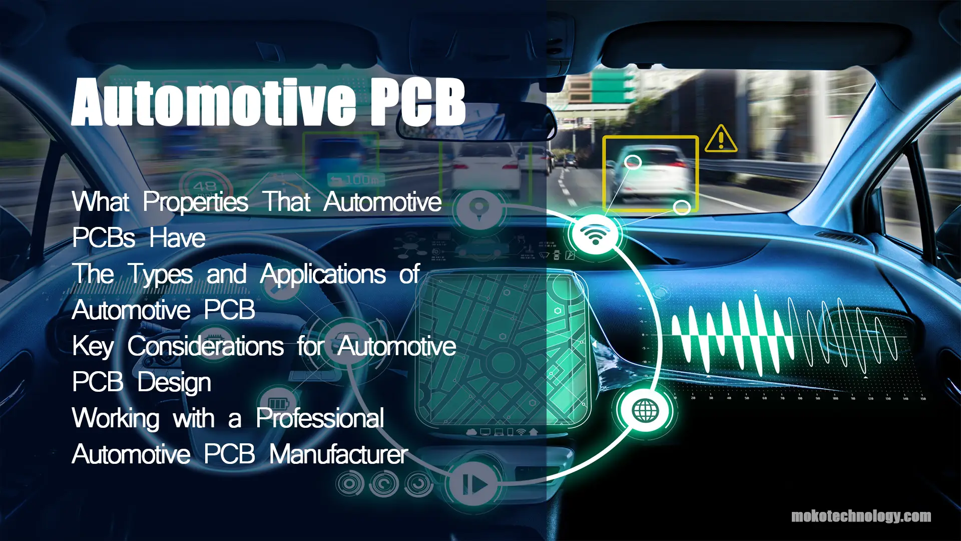
Samochodowe płytki drukowane są krytycznymi komponentami używanymi w różnego rodzaju samochodowych systemach elektronicznych, w tym systemy czujników, sterowanie silnikiem, GPS, systemy bezpieczeństwa, wyświetlacz cyfrowy, i oświetlenie LED. Jako elektryczny i
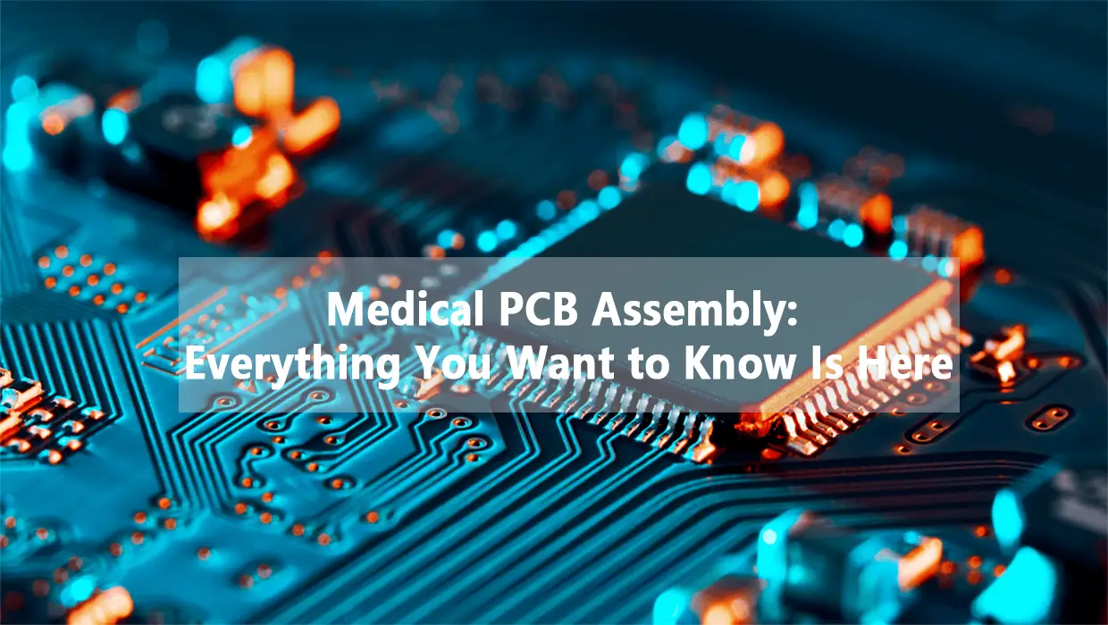
Medyczne PCBA jest szeroko stosowane w różnego rodzaju urządzeniach medycznych, takich jak urządzenia diagnostyczne, urządzenia monitorujące, urządzenia medyczne, i urządzenia do obróbki. W rzeczywistości, prawie każda elektronika medyczna wymaga użycia
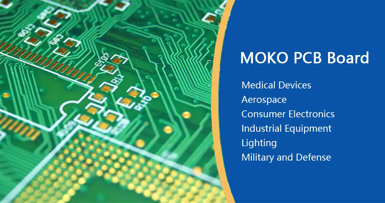
Co to jest płytka PCB? A PCB board refers to a board that provides an electrical connection for different components by using wires and conductors and offers mechanical support for surface-mounted and socketed
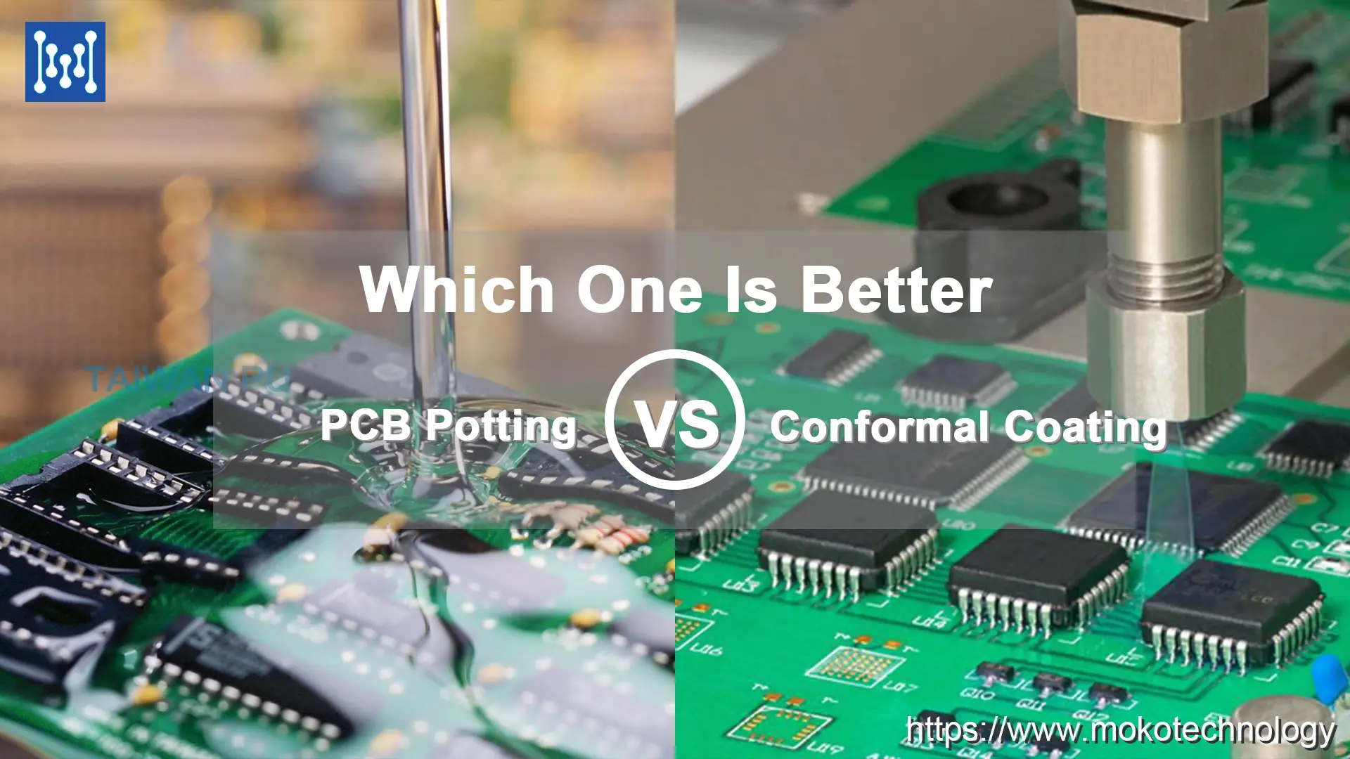
Dlaczego zalewanie lub pokrywanie konforemne jest konieczne w przypadku PCB? Zalewanie i powlekanie konformalne są niezbędnymi technologiami do produkcji PCB, które chronią PCB przed niekorzystnymi czynnikami, takimi jak wilgoć, chemikalia,
