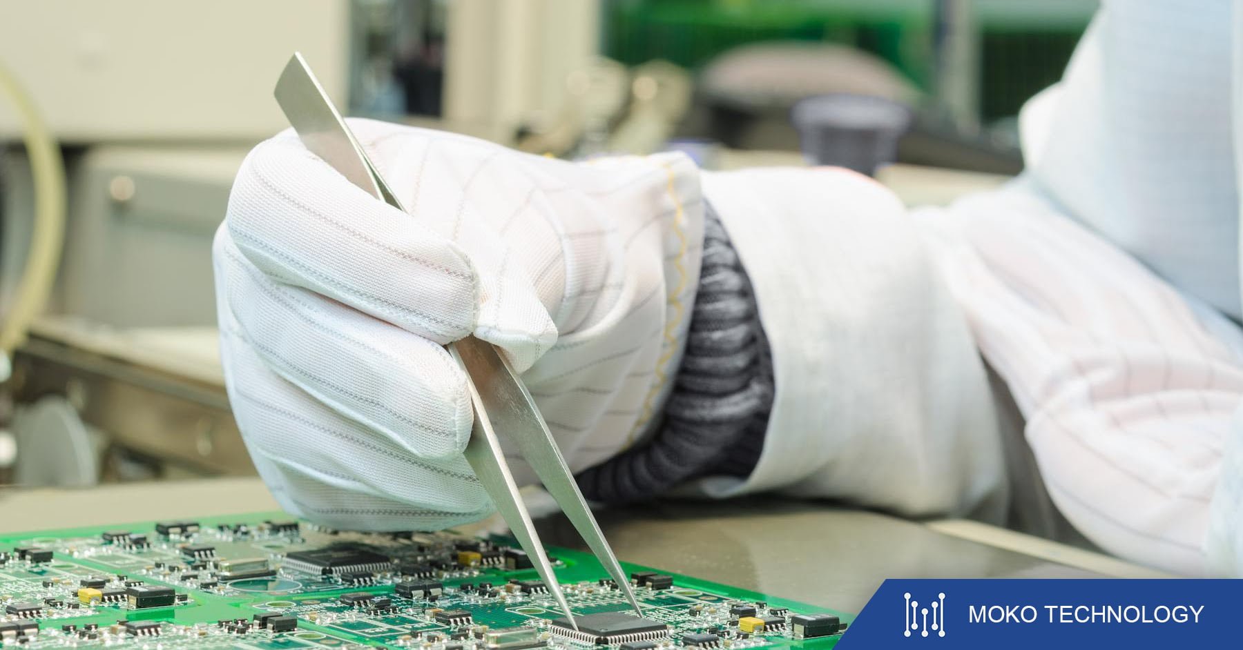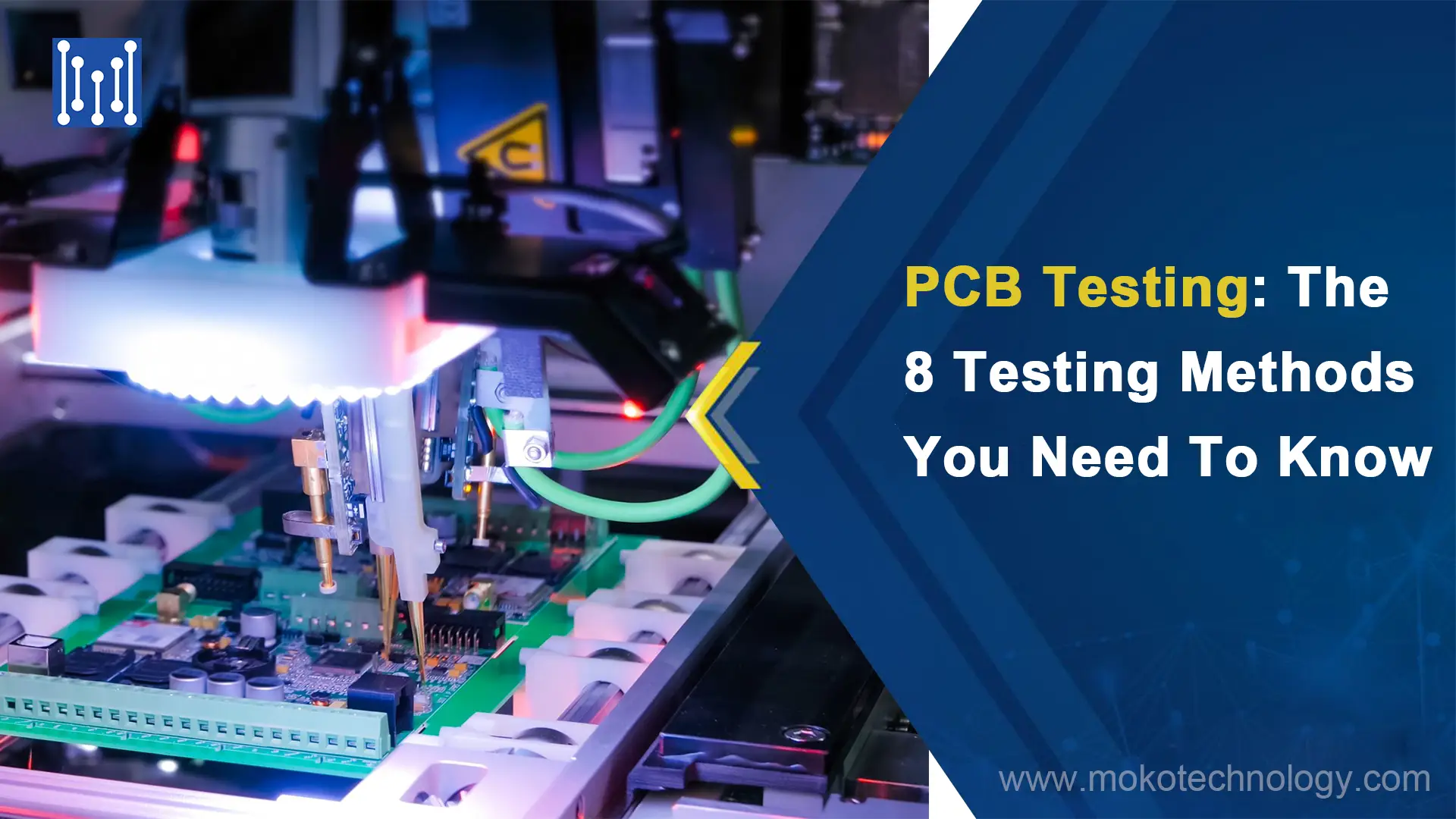
PCB testing is a crucial step in the PCB assembly process. Without proper testing, printed circuit boards may contain flaws that were overlooked during production.
Thorough testing helps catch errors and defects before the boards reach customers. This prevents field failures down the line and maintains customer satisfaction. There are several key testing procedures that should be performed to validate full functionality of both the bare PCB and assembled components. In this blog, we will explain 8 types of common PCB tests, let’s check them one by one.
8 Types of Common PCB Testing Methods
There is no specified method to use and perfectly test PCBs fully. Thus many factors should take into consideration when making a decision on which method to use. The key to this is to focus on the correct testing procedures, reliability, and the cost of testing. There are various methods to use in PCB board testing and designing to optimize the assembly process.
-
In-Circuit check (ICT)
Many PCB makers favor using one style of in-circuit testing (ICT) or another. Using ICT, a manufacturer will with efficiency check individual elements and their electronic characteristics.
Traditional ICT needs a “bed of nails” fixture. These fixtures should bear a style section to suit the circuit card. The fixtures generally come back at a nice expense. ICT shines best once used for end-of-line testing of largely stable, high volume productions. Once the assembly doesn’t justify the value, makers should generally pass a number of the fixture prices on to customers.
-
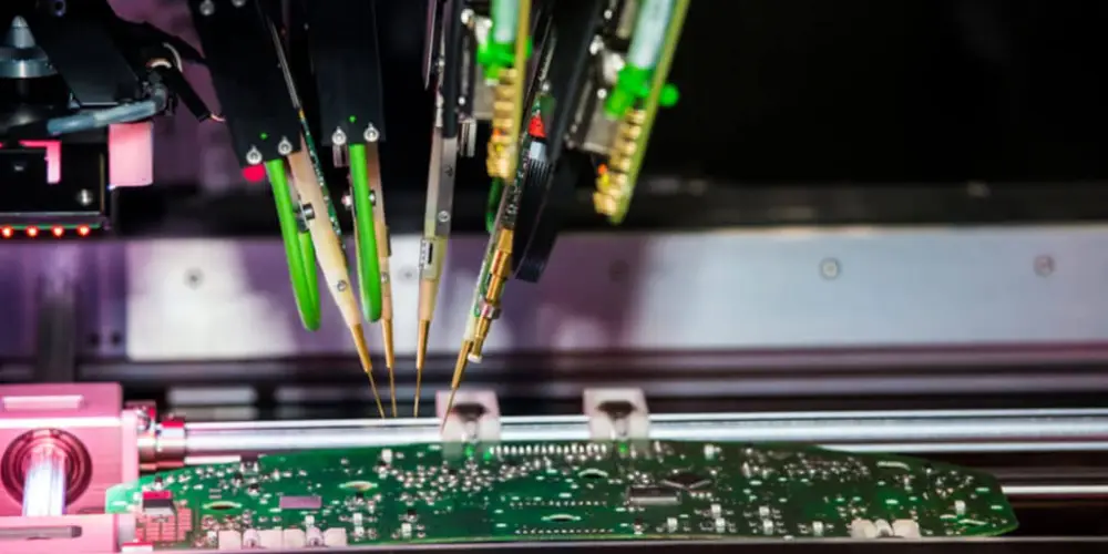
Fixtureless In-Circuit check (FICT) / Flying Probe Test
A flying probe test, conjointly called fixtureless in-circuit testing (FICT), is another style of ICT. Flying probe eliminates the requirement for custom fixtures that eliminates more fixture prices. FICT uses check pins that move supported programming (flying probes).
However, it has the advantage of cost accounting less and, therefore, the ability to check either side of a PCB. If a defect or downside shows up, the FICT system solely needs reprogramming to provide a brand new piece while not the defect? In contrast, and ICT will need a wholly new fixture. Programming guides the flying probes, which make it attainable to run tests that pinpoint extremely specific areas and nodes. That level of accuracy works well with smaller boards and boards with high-density elements.
-
Functional Circuit check
Functional tests area unit dead to certify that the electronic equipment functions in keeping with style specifications. Testing is often performed mistreatment DUT (device below test) connectors or a BON (bed of nails) fixture. A pogo pin device, a setup wont to establish a short-lived association between 2 computer circuit boards, is employed to conduct testing. The number of pogo pins, sometimes required for a practical check fixture, is considerably but associate ICT fixture.
-
Boundary Scan Testing
The boundary scan could be a methodology for testing wire lines on computer circuit boards. Boundary-scan is additionally wide used as a debugging methodology to look at computer circuit pin states, live voltage, or associate analyze sub-blocks within a computer circuit.
-
Automated Optical Inspection (AOI)
Automated optical inspection (AOI) uses cameras to visually scan PCBs and compare to the original design files. Any deviations beyond a set tolerance trigger manual inspection. AOI provides fast defect detection to avoid continued production of flawed boards. However, AOI has limitations in only checking physical features without powering up components. For comprehensive testing, AOI should be paired with additional methods like flying probe, in-circuit, or functional testing to validate performance. AOI is most effective as an initial screening tool combined with electrical verification.
-
Burn-In Testing
Burn-in testing intensely stresses PCBs to uncover early defects and establish load capacity. It continuously runs power at maximum specified levels through boards for 48-168 hours. Failures during this time are called infant mortalities. For military or medical devices where reliability is paramount, burn-in testing makes sense to avoid dangerous product launches. However, it can shorten lifespan if overstressed. If few defects appear, the test duration can be reduced to avoid overstress. Periodic reevaluation of burn-in protocols balances reliability assurance and lifespan impact.
-
X-ray Inspection
X-ray inspection, or AXI, examines PCBs for defects by producing internal images. 2D and 3D versions locate issues like poor solder joints, broken traces, and barrel cracks. 3D is faster. AXI reveals hidden flaws like under-chip ball grid array solder connections. However, it needs skilled operators to interpret the complex x-ray images correctly. While x-rays can penetrate multilayer boards, checking every internal layer is infeasible and costly. AXI balances defect detection and inspection time through selective imaging of critical components and layers. Periodic reassessment of AXI procedures optimizes this balance as designs evolve.
-
Visual Inspection
Visual inspection involves thoroughly examining a printed circuit board using optical aids to check for physical defects. Inspectors look for issues like missing or damaged components, poor solder connections, contamination, assembly errors, and board damage. Magnifiers, microscopes, and imaging systems are often used to get a closer look at the PCB surface and identify flaws difficult to see with the naked eye. Visual inspection serves as an initial quality control step to catch obvious manufacturing issues before further testing procedures.
Benefits of PCB Board Testing
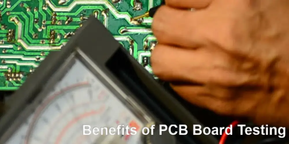
Bug identification: The main advantage of PCB testing is that it assists in identifying problems in PCBs. If the issue lies in manufacturability, functionality, or elsewhere, PCB board testing is able to identify what is a PCB design so that designers can regulate as a result.
Time savings: PCB testing serves as an early stage to help save time in the long run. The testing also allows designers to identify major issues during the prototyping stage. In the testing process enables designers to govern the root cause of each problem posed quickly and easily. It also leads to early decisions if to make adjustments so that they can move on with production at a faster rate as well as manage production time.
Cost reduction: PCB testing plays a key role in reducing wasteful production of faulty products by applying prototypes and small-scale assemblies to test the products. When testing is done early in the design process, it helps the designers to prevent wasteful full-scale assemblies of faulty PCBs. It also serves to ensure that the design is as flawless as possible before it goes into production. This step helps to reduce production costs meaningfully.
PCB Testing Tools
There are two key tools one can use to test if the PCB is functioning as intended. They are:
- Multimeter
A multimeter is incredibly helpful for measuring voltages, current, and resistance within a circuit. It allows validation of power levels, continuity, and basic functionality. Handheld digital multimeters provide portability for testing during assembly and troubleshooting.
- Oscilloscope/Logic Analyzer
Oscilloscopes and logic analyzers visually display changing voltage over time to observe circuit operation and signals. This waveform monitoring is essential for verifying timing, speeds, noise, and complex interactions in digital and analog circuits. Standalone oscilloscopes are costly, but DIY options exist using an Arduino, PC soundcard, and custom circuitry to achieve basic functionality at a fraction of the price. This can be a great addition for hobbyists and students wanting to add visual testing capabilities on a budget.
Other handy test tools include clip-on ammeters to measure current draws, LCR meters to quantify inductance, capacitance, and resistance, and thermal imagers to check hot spots on operating boards. Building up a toolkit of testing equipment tailored to the specific PCB project enables comprehensive validation during development and troubleshooting.
Choose MOKO Technology for PCB Testing
At MOKO Technology, we deeply understand the importance of comprehensive PCB testing and ensure our products are rigorously validated. With over 17 years of experience in the PCB industry in China, we have assembled a veteran team of manufacturing engineers and specialists dedicated to quality assurance. Our testing capabilities cover the full range of electrical, functional, and mechanical checks needed to verify design and reliability. For more information, contact the experts at MOKO today.