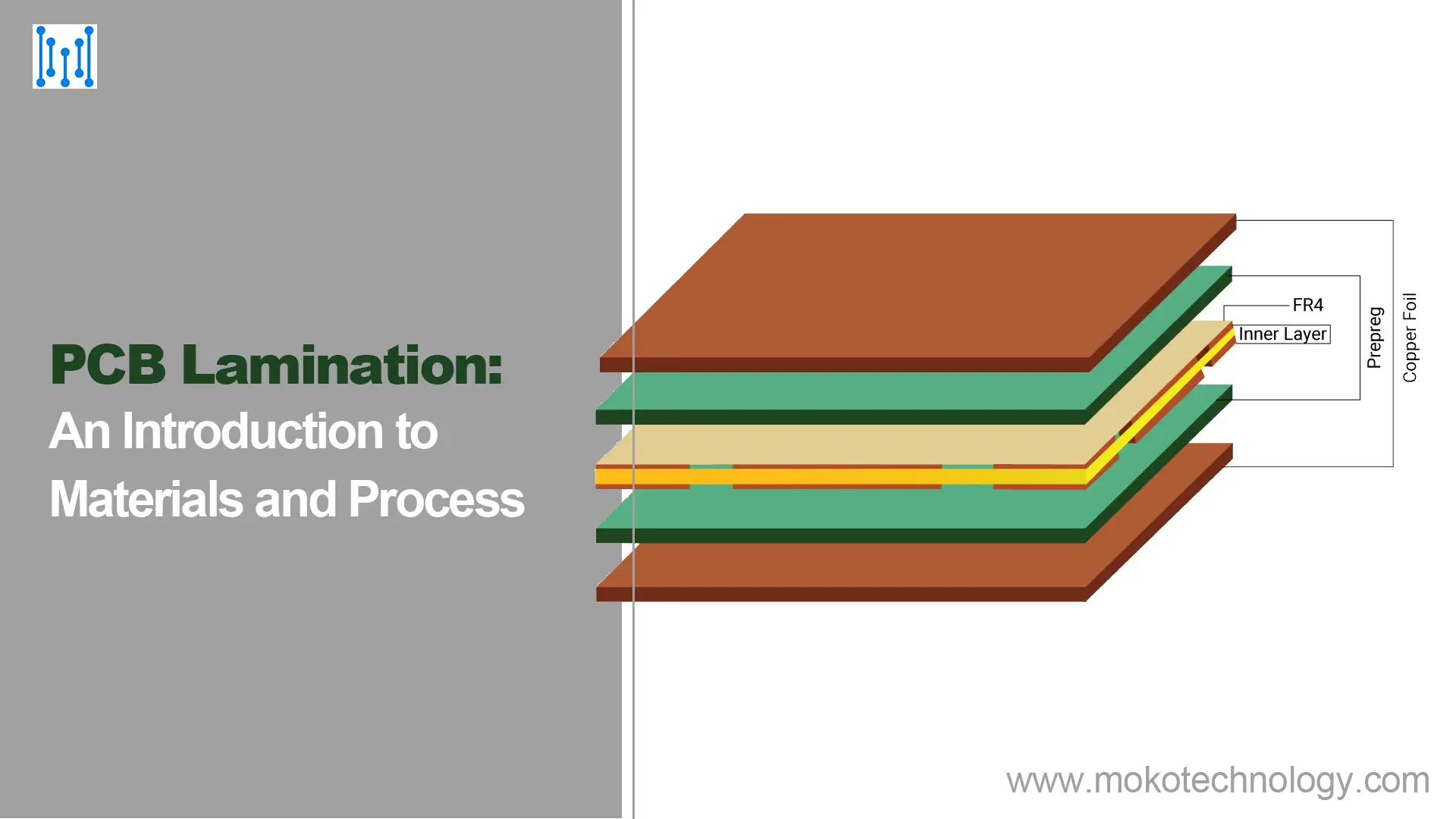
PCB lamination is a critical step in PCB fabrication, which involves “sandwiching” a core layer containing the circuitry between sheets of printed circuit board laminate material. Proper lamination is essential for creating a durable PCB that can withstand mechanical and thermal stresses during its lifetime.
So what exactly is PCB lamination and why does it matter? Lamination refers to the process of permanently bonding sheets of insulating material, known as laminates, to the conductive copper layers through the application of heat and pressure. This forms a multilayer board with the circuitry sealed safely within. PCB lamination is important because it provides structural rigidity and protects the copper from the environment, while also insulating between conductive layers to prevent short circuits.
In this beginner’s guide, we’ll explore the different types of laminates used in PCBs, walk through the lamination process step-by-step, and examine key factors to consider when selecting laminates. Let’s get started!
Different Types of Printed Circuit Board Laminates
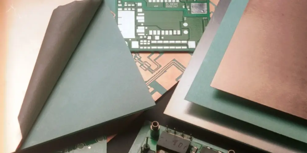
There are several types of laminate materials used for the insulation layers in a PCB. Some of the most common include:
-
FR-4 laminate
The most prevalent laminate material used today is FR-4, a glass fiber reinforced epoxy resin. This material offers a good balance of performance, cost, and availability. The woven fiberglass reinforcement provides mechanical rigidity and strength to the board. The epoxy resin system imparts electrical insulating properties and bonds the layers together when cured.
FR-4 circuit board laminates are available from many manufacturers in a range of glass weaves, resin contents, and weights. Electrical properties like dielectric constant can be tuned by adjusting the resin chemistry. The relative affordability and versatility of FR-4 make it suitable for many general circuit board applications.
-
CEM-1laminate
For more cost-sensitive applications, CEM-1 laminates may be used as a lower cost alternative to FR-4. CEM-1 uses a composite epoxy resin reinforced with cellulose paper rather than fiberglass.
Since cellulose paper fibers are not as strong as fiberglass, CEM-1 has reduced mechanical properties. It also absorbs more moisture. But the materials cost is substantially lower, providing some PCB cost savings when performance requirements are less demanding.
-
Polyimidelaminate
Polyimide films like Kapton provide excellent thermal stability and chemical resistance. This makes them suitable for flexible PCB applications. The repeated flexing of circuits requires robust laminates. Polyimide films can withstand very high temperatures, with glass transition temperatures over 300°C. This heat resistance allows polyimide-based flexible circuits to be applied in high temperature environments. Common applications include electronics in aerospace systems.
-
High Frequency/High Speed
Specialized printed circuit board laminates engineered for optimal electrical performance are used in high frequency PCB and high speed digital PCB. Key properties like dielectric constant and loss tangent are minimized to maintain signal integrity at faster speeds.
Common high frequency/high speed laminate materials include PTFE (Teflon) composites reinforced with microglass fibers. Ceramic-filled PTFE blends are also used. The precise dielectric properties can be tailored for target applications.
-
Metal Clad Laminate
Metal-clad laminates have thin foil layers of metal like copper or aluminum bonded to one or both sides of the dielectric substrate. This allows creation of metal core PCBs, which have the metal layer in the center to spread and dissipate heat.
Aluminum clad laminates provide the highest thermal conductivity for heat dissipation. Copper clad laminates also have good thermal properties. These metal-based boards are ideal for high power electronics where thermal management is critical.
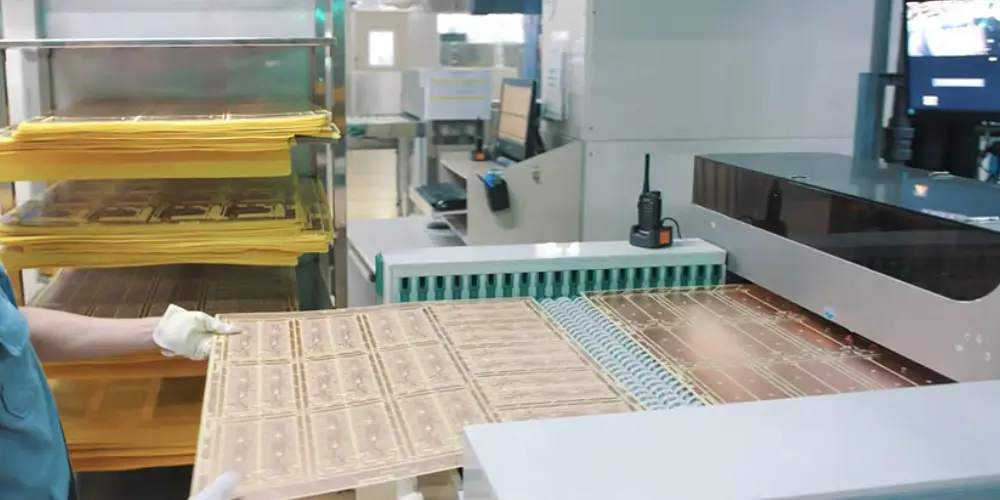
Step-by-step Explanation of PCB Lamination Process
- Surface Preparation
This process involves cleaning panels thoroughly, rinsing them with purified water, eliminating corroded copper surfaces and fingerprints, and removing residues
- Micro-etching
In micro-etching, a copper foil that has been previously plated is oxidized using acid. This method ensures uniformity in the copper layer and preserves specific areas, such as pads and routes, essential for transmitting electrical signals, without exposing them during the process.
- Surface Treatment
Utilizing a black oxide bath, the PCBs undergo a meticulous surface treatment, enhancing adhesion for epoxy resin and effectively averting delamination issues.
- Inner Layer Stack-up
At this point in the process, an operator carefully organizes the inner layers and prepregs in the correct sequence and gently bonds them together using the riveting machine.
- Full Stack Assembly
The assembled stack is sandwiched between sheets of copper foil and stainless steel plates. The steel plates prevent warpage and damage during lamination. This full assembly goes into the laminating press.
- PCB Lamination
The sandwich assembly enters a heated hydraulic laminating press. Under heat and pressure, the prepreg layers soften and flow while the epoxy cures. This bonds the layers into a solid laminated circuit board. PCB lamination typically takes 1 to 2 hours under heat and pressure.
- Cooling
After lamination, the cured assembly moves to a cooling press. Cooling under pressure prevents warpage and internal stresses from developing as temperatures drop.
- Detacking
The stainless steel plates are detached from the laminated board once it reaches room temperature. This exposes the outer copper foil layers.
- Hole Alignment
X-rays check inner layer hole alignment after lamination. Any shifting during the high pressure bonding process is detected. Holes are deburred and reamed until all layers realign, ensuring reliable connectivity between PCB layers.
Factors to Consider When Choosing Circuit Board Laminate
With an abundance of laminate options, it’s important to select the right material based on product requirements and PCB design considerations:
Quality Control-Require suppliers to provide documentation that their laminates use the right materials and meet all specifications. Review test reports and quality certs to confirm boards will meet performance needs.Dielectric Constant – The propagation speed of signals on a PCB laminate and impedance control are influenced by the dielectric constant. A reduced dielectric constant facilitates swift signal transmission in high-speed designs.
Loss Tangent – At high frequencies, the loss tangent dictates how much signal is lost due to absorption in the laminate material. A lower value in the loss tangent enhances overall signal integrity by minimizing signal loss.
Thermal Conductivity – It represents how quickly heat moves through the laminate. A higher thermal conductivity promotes effective heat dissipation from hot components on the board, ensuring optimal temperature regulation.
Coefficient of Thermal Expansion (CTE) – This coefficient signifies the laminate’s expansion with each degree rise in temperature. Aligning the CTE between the laminate and copper layers mitigates thermal stresses, enhancing the stability of the PCB.
Glass Transition Temperature (Tg) – Tg marks the point where the laminate transitions from a rigid to a softened state. To prevent overheating damage, the Tg should surpass the maximum PCB operating temperature by at least 50°C, ensuring the board remains structurally intact.
Surface resistivity- Verify the laminate’s surface resistivity falls within the ideal 103 to 109 megaohms per square meter range. Moisture and temperature affect values. Select laminates meeting requirements even under expected environmental conditions.
Final Thoughts
PCB lamination may seem like just a manufacturing detail, but it is a pivotal process in PCB fabrication. Using the right circuit board laminate materials and following careful lamination procedures helps produce reliable, high-performing circuit boards. For the best results, partner with a manufacturer that has expertise in laminate selection along with state-of-the-art lamination processes. With the basics covered in this beginner’s guide, you’re now ready to dive deeper and consider lamination an integral part of your next PCB design. For any further questions, feel free to contact with our PCB specialist.