Fiducial marks, also known as fiducials, are small copper markers printed on PCB that serve as visual reference points during assembly and inspection, allowing automated assembly machines and quality control systems to precisely locate specific features and components. PCB fiducial mark typically consists of circular pads or other exposed copper shapes surrounded by clearance areas. This guide introduces types of fiducial marks, explains their functions and design considerations, and aims to provide guidance for beginners in PCB design. Let’s dive in.
Types of PCB Fiducial Marks
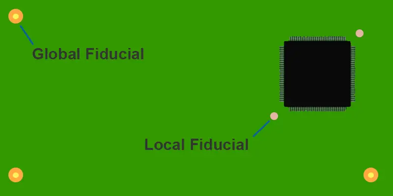
There are two main types of fiducials that are commonly used: global fiducials and local fiducials.
Global fiducials are reference markers placed along the edges of a PCB. They allow assembly machines to orient the board and determine its precise X-Y axis alignment. Global fiducials also enable the machines to compensate for any skew that occurs when the board is clamped down.
Local fiducials are placed near component footprints, especially for large or finely-pitched surface mount components. Local fiducials give the assembly machines exact reference points to locate each component footprint. This reduces errors and variability in placement.
How Fiducial Marks Work
Fiducial marks function as identification points on a PCB board, they provide alignment guides for PCB stencil positioning and automated pick-and-place component installation.
Automated machines utilize the fiducial mark locations during assembly to properly place the board. The measurements of these locations can serve as points of reference for the accurate placement of SMT components. The device utilizes image recognition to accurately identify the exact positions of fiducial markers on the PCB board each time an operator loads the board for printing or component installation. Subsequently, the machine autonomously adapts its positioning based on the fiducial marker information.
Benefits of Using Fiducial Mark
- Improve accuracy and precision inPCB assembly
Fiducials provide fixed reference points that assembly machines use for precise positioning and alignment. This improves placement accuracy of components compared to relying solely on the board edges. They enable precise alignment between the PCB and stencil in the process of solder paste printing. This improves print quality and reduces defects. Fiducials increase assembly precision across large PCB panels by accounting for any distortions.
- Reduce human errors
Automated assembly systems rely on fiducials for accuracy instead of human visual judgment. This reduces positional errors caused by operator variability. In addition, PCB fiducial markers eliminate the need to manually measure or mark component centres. This saves time and avoids human measurement errors.
- Aid in automated optical inspection
AOI systems use fiducials to digitally align inspected boards to the reference design. This enables detecting defects by comparing to the original design. Fiducials on PCB provide fixed scaling and measurement references for inspection cameras. This allows precise automated measurements of components, pads, spacings, etc. They enable effective rework by helping AOI cameras identify and highlight component positions requiring fix.
Guidelines on Incorporating Fiducial Marks in PCB Design

Proper PCB fiducial design will facilitate automated assembly and enhance quality control. Below are listed some key points when using fiducial marks:
- Fiducial marks should only be placed on the top or bottom copper layers of a printed circuit board because this exposes the copper for easy detection.
- The fiducial marks must remain uncovered by solder maskfor automated optical systems to identify them during assembly, since covering fiducials would obstruct machine vision tracking.
- High visual contrast between the fiducial copper and base board material aids recognition, so dark fiducials on a light background, or vice versa, are optimal.
- Keep fiducial diameters between 1-3 mm, with under 25 microns of size variation on a single board, because consistency enables precision calibration.
- For global fiducials, use at least 3 spaced across the PCB edges when possible, as this provides the best rotational alignment; at minimum, place 1 global fiducial.
- Local fiducials require 2 markers flanking surface mount component footprints in order to accurately locate the component positions.
- Position global fiducials at least 0.3 inches from board edges, excluding the fiducial clearance area, to prevent interference.
- On larger boards, spread the fiducials farther apart to better detect slight angular misalignments during fabrication.
Key Takeaways
Fiducial markers play a vital role in PCB design and manufacturing, despite their small size. They serve as guidepoints for assembly machinery to achieve precise alignment and component placement. Integrating fiducials into the PCB design has numerous benefits such as enhancing precision, minimizing errors during automated assembly, and optimizing manufacturing efficiency by facilitating machine processes.
By understanding the importance of proper fiducial placement and design, PCB fabricators can boost overall quality and performance. Following optimal fiducial strategies enhances the accuracy and effectiveness of electronic products. We hope this article has offered valuable guidance on PCB fiducial mark, particularly for those new to the PCB industry. Please reach out if you have any additional questions.