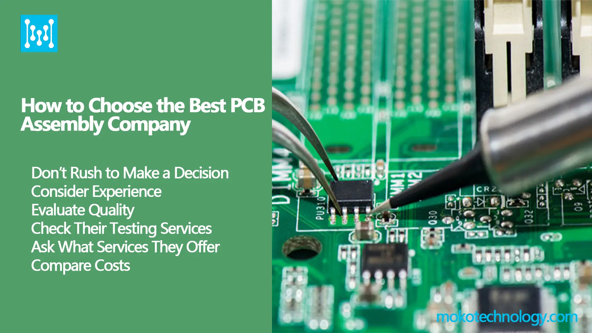
What Is PCB Fabrication
PCB fabrication refers to the process of manufacturing printed circuit boards (PCBs), which are essential components in electronic devices. PCB fabrication involves the creation of a physical board that provides the electrical connections between various electronic components, such as integrated circuits (ICs), resistors, capacitors, and connectors, in a compact and organized manner.
The PCB Fabrication Process
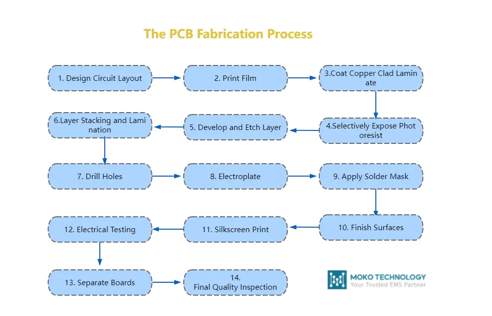
Step 1: Design Circuit Layout
The electrical circuit is designed in ECAD software. The layout data is converted into Gerber files containing coordinates for copper layers, solder mask, silkscreen, drills, etc. Design rule checks validate manufacturability.
Step 2: Print Film
A specialized photoplotter printer creates high resolution film negatives of each layer onto transparent plastic sheets coated with photosensitive emulsion. Registration holes precisely align layers.
Step 3: Coat Copper Clad Laminate
The raw PCB substrate is cleaned and laminated with a layer of photoresist. An adhesion promoter may be used to aid resist bonding.
Step 4: Selectively Expose Photoresist
The film negatives are carefully aligned to the laminate using registration pins. A UV light source selectively exposes the photoresist according to the layer image.
Step 5: Develop and Etch Layer
The board is immersed in chemical developer solution to dissolve away unexposed resist. Etchant removes copper not protected by resist to create conductor patterns.
Step 6: Layer Stacking and Lamination
Individual inner and outer layers are aligned using registration holes or a vision system. Layers of prepreg and copper foil are precisely stacked and laminated together under heat and pressure.
Step 7: Drill Holes
Holes for component leads and vias connecting layers are precision drilled using a computer numerical control (CNC) drill. Hole walls are deburred.
Step 8: Electroplate
A thin layer of copper is autocatalytically deposited onto all exposed surfaces to provide base conductivity for electroplating.
Step 9: Apply Solder Mask
Liquid photoimageable (LPI) solder mask is applied over the entire board and cured to protect copper traces from oxidation and prevent solder bridges.
Step 10: Finish Surfaces
Exposed copper is coated with hot air solder leveling (HASL), organic solderability preservative (OSP), immersion silver, or immersion gold.
Step 11: Silkscreen Print
Reference designators, symbols, company info, board outlines, and other markings are printed using silkscreen ink.
Step 12: Electrical Testing
Continuity, isolation testing, and in-circuit or flying probe testing verify there are no open or short circuits.
Step 13: Separate Boards
V-groove cutting, routing, or scoring separates individual boards from the larger panelized boards.
Step 14: Final Quality Inspection
Electrical, visual, and mechanical inspection ensures boards meet specifications before shipment.
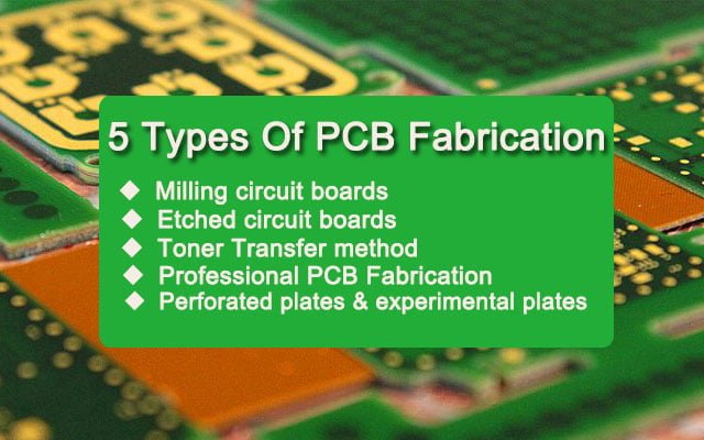
5 Types of PCB Fabrication Techniques
Now, let’s discuss different techniques for fabricating printed circuit boards, from DIY to professional production:
- Perforated plates and experimental plates
The easiest way of PCB fabrication is with so-called experimental plates. These are PCBs made of hard paper or epoxy resin (GRP), which are drilled with a pitch of 2.54mm (= one-tenth of an inch). The copper layer is either just around these holes as pads or as strips. This means that smaller circuits can be set up quickly. The components are inserted on the side without copper and soldered on the other side. Connections can be made with thin wires and strands. However, this type of printed circuit board does not satisfy in the long run. It just looks too much like “handicrafts”.
- Milling circuit boards
Another option for PCB fabrication service is to take a copper-clad board and mill conductor tracks on it. A drill stand and a small, fast-running drill are sufficient. Corresponding conductor tracks can be milled freehand or with a stop using a small, pointed cutter. The holes for the components are then drilled.
While this option is available for long, straight conductor tracks – such as passenger car lighting – the limit of what is possible is quickly reached with more complex PCB boards. In addition, it takes a lot of flair to mill paths freehand. This method can therefore only be used to a very limited extent unless you have a milling cutter with a motorized XY table.
- Etched circuit boards
PCB etching involves selectively removing copper from a substrate to form circuit traces. First, the circuit layout is designed and mapped onto a copper laminated board. The board is then prepared for etching by using a resist material, like a waterproof ink or toner, to protect the traces. The board is dunked in an etchant solution which removes the unwanted copper not protected by resist. Afterwards, the resist is removed and a solder mask applied. Finally, holes are drilled to complete the PCB. Etching allows DIY prototyping but manual methods have limitations in trace width and production volume. For manufacturing, more advanced photolithographic processes transfer the layout with precision onto boards. Etching then selectively removes copper according to the layout to efficiently produce quality circuit boards.
- Toner Transfer method
The toner transfer method prints a mirror image layout onto coated paper using a laser printer. The toner is then transferred to a cleaned copper board by heat pressing with an iron, creating a resist pattern for etching. Alternatively, toner can be chemically transferred using magazine paper and nail polish remover as the solvent. Both methods allow hobbyists to produce precise PCBs with thin traces at home. The boards are then etched to remove exposed copper, leaving the desired traces protected by the toner
- Professional PCB Fabrication Service
Instead of making PCBs yourself, you can send your design files to a professional PCB manufacturer. They use advanced processes like photolithography to produce professional quality boards with very fine features. The detailed process is mentioned above. This is ideal for mass production or complex multilayer boards. This is a service offered by specialized companies that use industrial-grade processes for manufacturing high-quality, production-grade PCBs. These services are suitable for mass production or when precise and reliable PCBs are required.
In summary, the first three are home PCB fabrication techniques, toner transfer is an amateur method, while professional fabrication services are used to produce production grade PCBs using industrial processes.
What Is the Standard for PCB Fabrication?
- IPC Standards
The Association Connecting Electronics Industries (IPC) is a leading organization that sets standards for the electronics manufacturing industry, including PCB fabrication. IPC standards cover various aspects of PCB design, manufacturing, and assembly. Some of the relevant IPC standards include IPC-A-600, IPC-2221, and IPC-6012.
- UL Certification
Underwriters Laboratories (UL) provides certification services for PCBs to ensure they meet safety and performance standards. UL certification is often required for PCBs used in critical applications, such as consumer electronics and electrical products.
- ISO Standards
The International Organization for Standardization (ISO) has various standards related to PCB fabrication, including ISO 9001 and ISO 14001. These standards address quality control, environmental responsibility, and process management in PCB manufacturing.
- RoHS and REACH Compliance
Regulations such as the RoHS and REACH in the European Union restrict the use of certain hazardous materials in PCBs and electronic products. Compliance with these regulations is crucial for global PCB manufacturing.
- J-STD Standards
The Joint Electron Device Engineering Council (JEDEC) publishes standards related to the electronics industry, including PCB assembly and soldering. J-STD-001 and J-STD-002 are examples of standards that address soldering processes and requirements.
Partner with a Reliable PCB Manufacturer
Crafting printed circuit boards is a highly intricate process where even the smallest blunders can translate into costly mishaps for businesses. So, when you’re in the market for a PCB fabrication partner, it’s wise to seek out manufacturers with a well-established history of reliability. MOKO Technology, with nearly two decades of hands-on experience in PCB fabrication and assembly, not only offers superior products but also prides itself on speedy turnarounds. Don’t hesitate; reach out for a PCB service quote today.