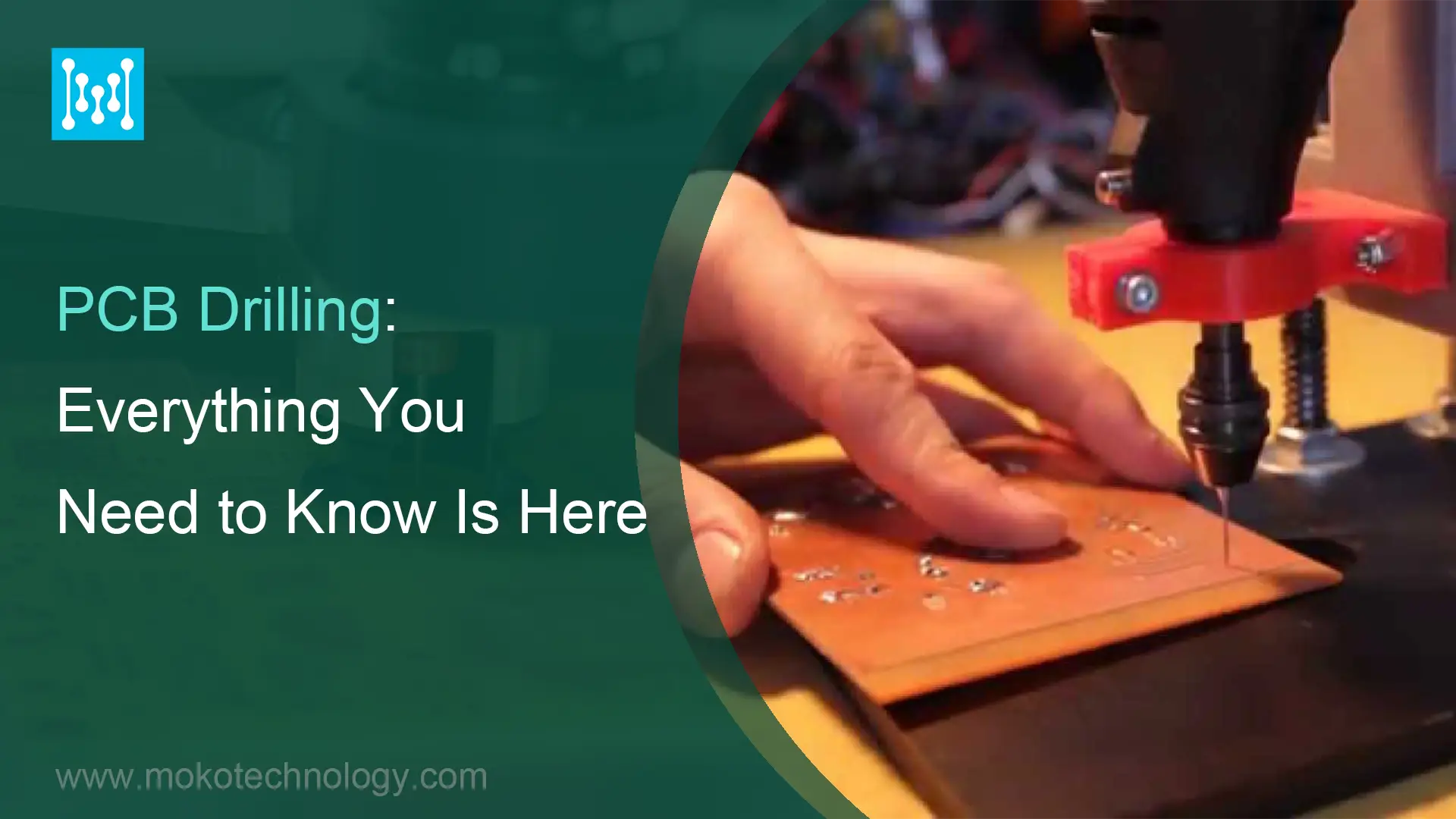
PCB Drilling: Everything You Need to Know Is Here

PCB drilling is an indispensable and intricate step in the overall PCB manufacturing process, serving as a fundamental pillar for achieving high-quality and reliable circuit boards. By creating precise holes and vias on the PCB substrate, drilling enables the intricate interconnection of electronic components, ensuring seamless communication and optimal electrical conductivity.
With advancements in technology, PCB drilling has become increasingly crucial in meeting the demands of modern electronics, where compact and efficient designs are imperative to accommodate complex circuitry within a limited space. It enables the realization of miniaturized devices, such as smartphones, tablets, wearables, and IoT devices, by providing the necessary connectivity and versatility. In this comprehensive guide, we will provide an overview of PCB drilling, covering its definition, different types, and useful tips, aiming to enhance your understanding of this crucial technology.
What Is PCB Drilling?
PCB drilling is the process of creating holes, slots, and additional voids in printed circuit boards according to the specifications of the board’s design. This operation is commonly executed through mechanical drilling techniques such as drilling, laser cutting, or punching, or through electrochemical etching (chemical milling). These drilled holes allow components like integrated circuits, resistors and capacitors to be mounted and soldered to the board. Overall, PCB drilling is a critical fabrication process that produces the holes needed to assemble electronic components onto printed circuit boards.
Two Commonly Used PCB Drilling Techniques
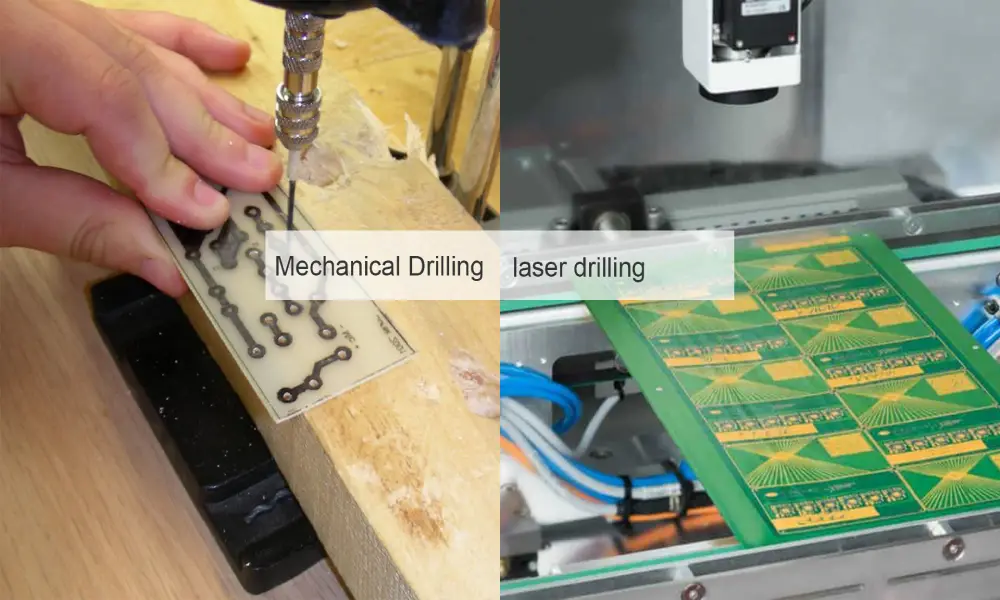

Mechanical drilling and laser drilling are two commonly used methods for printed circuit board drilling, and each of them has its advantages and considerations, by understanding the different PCB drilling techniques available, manufacturers and designers can make informed decisions to optimize their fabrication processes and achieve high-quality PCBs that meet specific design requirements.
Mechanical Drilling
Mechanical drilling involves the use of drills, typically made of tungsten carbide, to create holes in the board substrate. This method offers versatility and can handle various board materials, including rigid, flexible, and multilayer PCBs. Mechanical drilling can achieve precise hole sizes and depths, making it suitable for high-density designs. It is a cost-effective and efficient process, commonly performed using automated drilling machines.
Laser Drilling
Laser drilling has gained popularity in recent years as a precise and efficient method for PCB drilling. It utilizes a laser beam to selectively remove material and create holes in the board. This drilling method offers high accuracy, allowing for smaller hole sizes and intricate designs. It is particularly advantageous for drilling blind and buried vias in multilayer boards. Laser drilling is a non-contact process that reduces the risk of mechanical damage to the PCB, making it suitable for delicate substrates.
Different Holes Drilled in a PCB
Various types of holes are drilled in a printed circuit board, which includes cut-outs, slots, and shaping features. Holes play different roles and can be categorized into three classes:
Via Holes
Via holes, which are small holes plated with metal, are used for transmitting electrical signals, power, and ground connections between different layers of the PCB. There are different types of via holes based on specific requirements:
Through-hole vias extend from the top to the bottom of the board, connecting traces or planes across various layers.
Buried vias are contained within the inner layers of the PCB and do not extend to the surface layers. They occupy less space and are suitable for high-density interconnect boards, but they are more expensive to create.
Blind vias start from the surface layers and only go partially through the board. They are costlier to manufacture but provide more routing space. Their shorter barrel can improve signal quality for high-speed communication lines.
Micro vias are smaller holes created using laser machines. They are typically two layers deep and are suitable for high-density interconnect boards or fine-pitch components like BGAs, requiring insertable escape vias.
Component Holes
Component holes are used for mounting components on the PCB. While surface mount parts are commonly used, through-hole packages are still preferred for certain components such as connectors, switches, and mechanical components that require robust mounting. Through-hole packages are also suitable for power components like resistors, capacitors, op-amps, and voltage regulators due to their ability to handle higher currents and heat dissipation.
Mechanical Holes
In addition to electrical components, a PCB may require holes for mounting mechanical objects such as brackets, connectors, and fans. These holes are primarily used for mechanical purposes, although they can be plated with metal if an electrical connection to the PCB is needed, such as for chassis grounding.

Common PCB Drilling Problems and Their Solutions
- Delamination
Cause – Delamination occurs when the layers of the PCB separate or peel at the drilled hole locations. It can weaken the PCB’s structural integrity and affect its performance.
Solution: Control drilling parameters to minimize heat generation, as excessive heat can contribute to delamination. Ensure proper preparation of the PCB substrate to enhance adhesion and prevent delamination issues.
- Smeared Holes
Cause – Excessive friction and heat generation around the drill bit softens the copper and causes smearing around the hole.
Solutions: Smeared holes can be prevented by using lubricants during drilling to keep drill bits cool and reduce friction. Slowing down the drilling speed and feed rate reduces heat build up around the bit. Carbide drill bits, which withstand heat better than high speed steel, can also be used.
- Rough Hole Walls
Cause – Using dull or worn out drill bits that tear rather than cut the material cleanly.
Solutions: Drill bits should be replaced at first signs of wear to maintain sharp cutting edges. Slowing the drill speed and using lubricants will minimize tearing. For best results, brand new drill bits can be used for the final PCB holes.
- Burrs
Cause – As the drill exits the hole, excess copper from the hole wall tears and sticks to the edge.
Solutions: Burrs can be removed by manually deburring with a tool, using an automated deburring machine, drilling at higher speeds to fracture the burrs, or applying high pressure lubricant during drilling to minimize their formation.
- Copper Dragging
Cause – Friction between drill flutes and hole wall causing copper to tear away.
Solutions: This problem can be minimized by increasing the spindle speed to reduce friction heating, lowering the feed rate so the drill does not bite too aggressively, using lubricants, and utilizing specialty drill bits designed to cut rather than tear the material.
- Poor Location Accuracy
Cause – Drill press feed/speed parameters need adjustment or drill bits wander.
Solutions: The PCB should be secured, the center punch used for pilot holes, feed rate and speed optimized for the material, and drill bits checked for wobble and replaced as needed. Drill stops can also improve depth consistency.
- Cracks Around Holes
Cause – Too much downward force exerted by the drill press.
Solutions: Reducing the feed rate and drilling pressure prevents this. Sacrificial support plates underneath the PCB can help. Drill bits should not be overtightened in the chuck either, as this can lead to cracking.
Final Thoughts
PCB drilling is a precise and time-intensive procedure that demands meticulous attention and caution. Even minor mistakes can result in significant losses. Therefore, it is essential to seek out a reputable and skilled PCB manufacturer. With over a decade of expertise in PCB manufacturing service, MOKO Technology has established itself as a trusted provider. Throughout the years, we have delivered precise and high-quality printed circuit boards to customers around the world. If you require professional assistance with your drilling needs, don’t hesitate to talk to our experts today.


Recent Posts
Impedance Matching: A Critical Factor in High-Speed PCB Design
Impedance matching has become a cornerstone of the signal integrity in the realm of high speed PCB…
How to Clean a Circuit Board Safely and Effectively?
It is important to learn how to clean a circuit board properly if you’re working…
Counterbore vs Countersink: Which to Choose for Your PCB?
When designing PCBs, selecting the appropriate type of holes for fasteners is crucial. And much…
PCB Copper Foil: Types, Properties & How to Choose
PCB copper foil is one of the most critical materials in the printed circuit board…
MOKO Technology Launches Vietnam Manufacturing Base in February 2025
Shenzhen, China - February 11, 2025 - MOKO Technology, a leading global electronics manufacturing service…
PCB Solder Mask: What It Is and Why Every Circuit Board Needs It?
While most people focus on the components and copper traces that make up PCBs, there's…