The space of printed circuit boards (PCBs) is often at a premium in modern, compact product designs, optimizing PCB size has become an essential consideration. Printed circuit board size impacts manufacturing costs, product dimensions, and even performance factors like signal integrity. While standard PCB sizes exist for common applications, customizing and minimizing the size of your board offers many advantages. This guide covers key factors in determining and reducing circuit board size.
Factors that Determine PCB Size
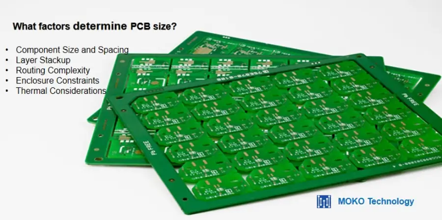
The ultimately achievable PCB board size depends on multiple design factors:
Component Size and Spacing – The dimensions of mounted parts along with minimum clearance rules dictate the basic PCB area. Larger components like connectors or quad flat packages and their spacing form the starting point for sizing.
Layer Stackup – Increasing PCB layer count enables denser routing across multiple layers, shrinking the board’s footprint. However, each added layer increases costs proportionally, so 4-6 layers offers a cost-effective balance.
Routing Complexity – Dense, compact routing of traces between closely spaced pads often determines the smallest achievable PCB board size. Autorouters excel at optimizing complex layouts.
Enclosure Constraints – The PCB must fit inside the product’s enclosure, so allotted space for connectors and components reduces the available area for the board itself.
Thermal Considerations – An adequate PCB area helps conduct heat away from components. Thermal needs may limit shrinkage, but careful design using vias, ground planes, and heat sinks can mitigate issues.
Many other factors like electromagnetic interference (EMI) shielding, panelization requirements, and serviceability influence size but can be balanced through careful PCB design.
Techniques for Optimizing and Minimizing PCB Size
A number of best practice strategies can help meet the challenge of PCB miniaturization:
- Component Placement
Parts performing similar functions should be clustered together when possible. Strategic placement also involves allocating the most space-constrained high-density parts first, ensuring they fit efficiently without excess unused space.
- High-Density Packages
Tiny micropackages such as 0201 and 01005 chip resistors, capacitors, and ICs take up a fraction of the real estate compared to 0402, 0603, or larger equivalents. The extensive availability of these miniature surface mount device (SMD) components is driven by the ultra-compact nature of consumer electronics. These parts can replace less efficient legacy options.
- Routing Channels
Shrinking the width of routing channels between component rows and columns allows traces to run more compactly between parts. However, this technique necessitates additional board layers to provide adequate routing capacity. Careful channel sizing balances routing density versus manufacturability.
- Trace Widths
By reducing copper trace widths, less space is consumed while routing interconnections. However, the designer must consider resistance and current capacity effects. Traces under 0.2mm are common for maximizing routability on high-density boards.
- Manual Layout
Autorouters deliver an initial routing arrangement, but critical space-saving PCBs require an expert layout designer to manually optimize the traces. This meticulous tweaking of trace paths extracts every bit of routing efficiency.
- Layer Stackups
Increasing the layer count avails more routing flexibility to condense layouts 6 layers or more are frequently required to effectively minimize dimensions. But each added layer increases costs.
- 3D Construction
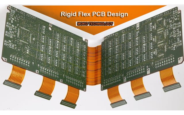
Innovative rigid-flex PCB technology allows folding 2D boards into efficient 3D shapes. The additional cost of these boards can enable greater functional density and compact enclosures. Careful 3D planning is required.
Benefits of Smaller Printed Circuit Boards
Shrinking PCB dimensions within functional limits carries numerous advantages:
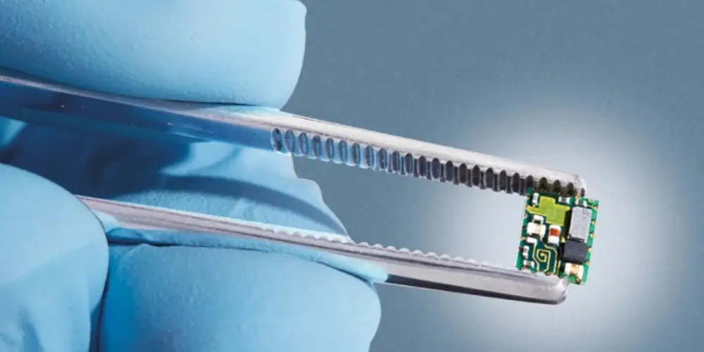
More Compact Products –By enabling significant miniaturization of printed circuit boards, smaller and more portable consumer gadgets can be designed, an important advantage for mobile devices like cellphones. Compact PCBs also conserve space in instruments and other electronics.
Lower Materials Cost –With the reduced board area of a smaller PCB, less substrate material and copper foil are required in fabrication, lowering expenditures on these materials. Fewer layers and shorter trace lengths also save substantially on materials costs.
Better Signal Integrity – Shorter trace lengths on a miniaturized printed circuit board lessen interference and signal distortion, allowing for cleaner and faster high-speed signal transmission critical for quality device performance.
Simplified Assembly – A key benefit of smaller PCBs is the ease of hand-soldering assembly, feasible with a reduced board size. Automated assembly also becomes faster and more efficient with less board area to populate components on.
Challenges with Miniaturized PCBs
The downsides of maximizing PCB compactness include:
- Complex Routing
Shrinking board dimensions significantly complicates routing dense copper traces between tightly-packed components with little space, often necessitating additional layers or highly skilled layout engineering to successfully interconnect all devices.
- Thermal Issues
Miniaturized PCBs concentrate heat generation into a smaller area with less surface for dissipation, challenging thermal management. Careful engineering of ground planes, thermal vias, heat sinks, and airflow is crucial to prevent overheating.
- Assembly Difficulty
The extremely small components and tight spacings on a compact PCB impede hand soldering and assembly, increasing difficulty and errors. Rework of faulty solder joints also becomes very challenging at a reduced scale.
- High-Frequency Losses
Excessive reduction of trace lengths can counterintuitively raise resistive signal losses at microwave frequencies above a few gigahertz, limiting miniaturization for high-frequency radio applications.
Conclusion
With rising compactness demands across electronics fields, PCB size optimization leverages minimum footprint designs that balance cost, performance, and manufacturability tradeoffs. Challenging yet achievable through careful component selection and layout, right-sized PCBs enable the levels of miniaturization that drive innovation. Both application-specific custom dimensions as well as pushing the limits of standard sizes offer advantages over one-size-fits-all thinking. As PCBs continue shrinking, engineers can meet size constraints through strategies like multilayer stackups, advanced routing, and 3D integration when needed.