In de PCB-productieproces, PCB warpage is a common problem that manufacturers would encounter. When a printed circuit board experiences warping, its performance and reliability would be affected. The warpage can cause many issues such as component misalignment, poor soldering quality, and even device malfunctions. Daarom, for PCB manufacturers and PCB designers, it’s critical to fully understand this issue. In deze blog, we will explain what causes PCB warping, and more importantly how to prevent such problem. Laten we verder lezen.
What Is PCB Warpage?
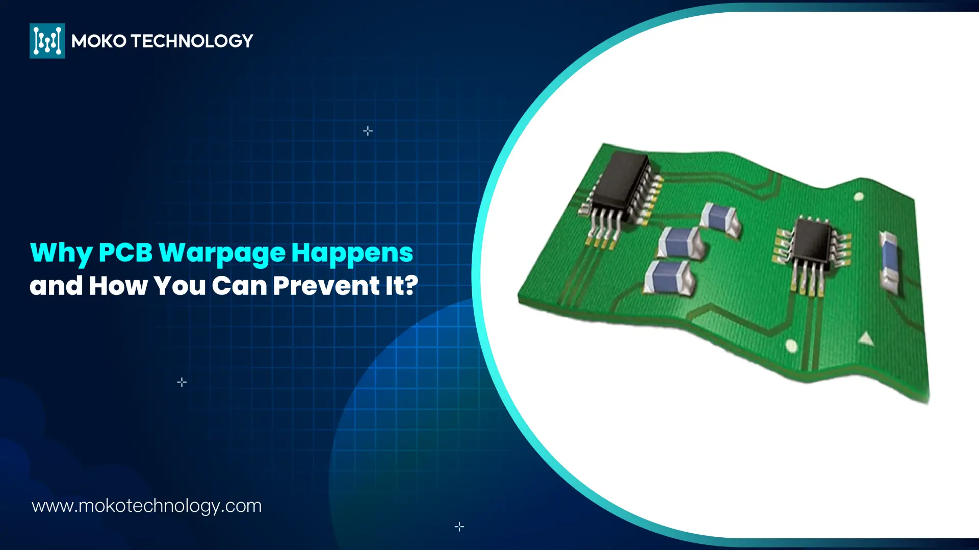
PCB warpage is a defect where PCB boards become distorted or bent out of its original flat shape. It can happen at the bare PCBs and also finished PCBAs. But in fact, every PCB will have a slight warp, which is inevitable during the lamination process in PCB fabrication. As for this issue, there are IPC standards including IPC-6011 and IPC-6012 that specify acceptable PCB warpage level. And they also set different classes that have different maximum warpage allowance:
| Klasse | Maximum Warpage Allowance | Example for a 400 mm long PCB |
| Klasse 1 | tot 0.2% of PCB length warpage | warped up to 0.8 mm |
| Klasse 2 | tot 0.15% of PCB length warpage | warped up to 0.6 mm |
| Klasse 3 | tot 0.1% of PCB length warpage | warped up to 0.4 mm |
| Klasse 4 | tot 0.05% of PCB length warpage | warped up to 0.2 mm |
How to Measure PCB Warpage?
Er zijn 5 commonly used methods to measure warpage in PCBs:
- Feeler Gauge Method
Use feeler gauges to measure warpage between high and low points of the warped PCB. This is usually used for large warpage values.
- Height Gauge
In deze methode, we need to use a mechanical or digital height gauge to measure height difference between high and low points, which allows us to get an accurate result of the warpage in inches or millimeters.
- ContourGauge
A contour gauge is used to trace the shape of the warped PCB. By placing the gauge on the surface, it adjusts to match the board’s contour, allowing for a visual or measured assessment of the warpage. This method is particularly useful for irregularly shaped warpage.
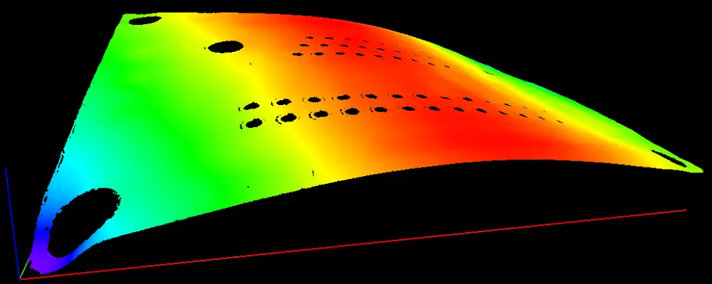
- Optical Profilometer
This method provides highly accurate measurement, which utilizes the optical profilometer to scan the warped PCB and then create a 3D profile of the PCB surface. Vandaar, we are able to identify even minute deformations of the board.
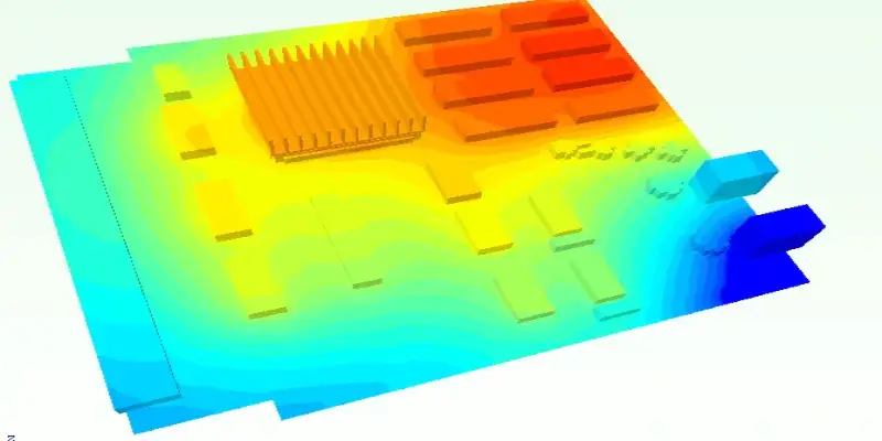
- Finite Element Method (FEM)
The finite element method is a computational approach that can simulate and analyze PCB warpage under various stress conditions. By inputting material properties and environmental factors, FEM predicts potential warping and helps manufacturers design PCBs with minimal deformation risks.

Main Causes of PCB Warping
- Stackup Asymmetry
Asymmetrically arranged PCB layers would cause PCB warpage. In dit geval, thermal stresses won’t be distributed evenly across the board during the heating process. Als gevolg, the PCB board will be warped or bent after cooling.
- Uneven Copper Distribution
A warped PCB can result if the copper in each layer is not distributed evenly. In a PCB, significantly more or less copper on one side than the other can lead to uneven expansion, causing warpage.
- Material Incompatibility
Different materials have different coefficients of thermal expansion (CTE) and Tg, which expand and contract at different rates during heating and cooling. This uneven stress causes the board to warp, especially during temperature changes in processes like reflow soldering.
- Improper Board Handling
If you clamp a board too tightly during wave soldering or reflow soldering, you may cause warping. When a clamped board is heated, it needs to expand naturally. If you clamp it to prevent expansion, the board may become permanently deformed, especially if it has heavy components that need to be soldered.
Further reading: Golfsolderen vs.. Solderen met reflow: Wat is het verschil?
- Poor Process Control
During the PCB manufacturing process, temperature cycling at various steps causes the circuit board material to expand and contract repeatedly. Excessive temperature cycling or improper process control can lead to severe warpage problems.
How to Prevent PCB Warpage?
- Thermal Management Techniques
We can reduce the possibility of PCB warpage by implementing effective thermal management techniques. Bijvoorbeeld, optimizing the reflow soldering profiles to minimize thermal gradients to ensure even heating and cooling. Bovendien, incorporating thermal relief features in PCB designs to dissipate heat more effectively.

- OptimizedPCB Design
During the PCB design process, ensure balanced component placement, and optimized trace routing is critical. Beside, we should use symmetrical interlayer prepregs and equal copper areas on both sides of the board to maintain uniform thermal distribution, so as to prevent PCB warping.
- Materiaalkeuze
When choosing materials, it’s essential to choose ones with compatible thermal and mechanical properties, which can minimize the risk of PCB warpage. For substrate materials, consider using FR4, since it offers good stability. Daarnaast, thinner substrates is better as they have less possibility of deformation.
- Uniform Copper Distribution
Making sure the copper foil is evenly distributed on both sides of the PCB, which is helpful to maintain the consistent heat conduction and prevent the PCB warping. Complementary layers should have similar copper coverage, which may involve using copper pour to fill unused areas on one side. When doing so, it’s important to define proper clearances in the design rules, especially if the filled layer needs to support controlled impedance.
- Bake PCBs beforeAssembly
Before assembly components, baking the bard PCB board is a critical step. This process can remove the moisture from the board, aan de andere kant, it helps fully cure the resin the laminate and reduces residual stress, so as to reduce the risk of circuit board warpage.
- Proper Storage
Avoid stacking and storing panels properly can also prevent PCB warping. The storage environment should be dry, and temperature-controlled. Panels should be stored flat with adequate support to prevent bending or deformation during storage.
Can PCB Warpage Be Fixed?
Once PCB warping occurs, it is often difficult to completely “fix” the warping, especially when the problem occurs on a finished bare board or PCBA. While some minor warping can be corrected by reflowing or baking the board under controlled conditions to reduce internal stresses, severe warping is usually irreparable, necessitating replacement. Daarom, rather than spending energy trying to fix a batch of warped PCBs, it is better to investigate the root cause and prevent the situation from happening again.
Laatste gedachten
PCB warpage is a prevalent challenge during the electronics manufacturing process. It’s difficult to fix once it occurs, but it can be prevented by identifying the root causes and implementing key measures, as mentioned above. MOKO-technologie, an experienced PCB and PCBA manufacturer with nearly 20 jarenlange expertise, produces high-quality boards that comply with IPC and ISO standards. We guarantee that the boards we deliver to our clients are free from warpage issues. Neem vandaag nog contact met ons op to discuss your PCB project and get a free quote!


