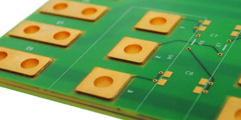
De kopersporen op een printplaat dragen elektronische signalen over en verdelen de stroom tussen componenten en apparaten. This complex network of conductive pathways allows all the functional elements on the board to operate in harmony. One of the most important design decisions when engineering a PCB is determining the appropriate PCB copper thickness for the traces. In dit artikel, we’ll look closely at the common copper thicknesses used in PCBs, discuss why utilizing thicker copper is advantageous in high power applications, and go over the key factors designers must consider when selecting the optimal circuit board copper thickness for their particular circuit requirements and constraints. Laten we erin duiken.
Common Copper Thicknesses Used in PCB
Copper thickness refers to the weight of the copper foil laminated onto the PCB-substraat, expressed in ounces per square foot (oz/ft2). Typical weights range from 0.5 oz to 3 oz:
0.5-1 oz copper thickness: An extremely thin copper foil at 0.0007 inches thick. Used for lightweight, low current PCBs where tight trace spacing and thin board profile are needed. The minimum trace size and spacing are very small with one ounce copper thickness.
1-2 oz koper: The standard and most common copper weight for general PCB designs. It provides a balance of electro-thermal performance and manufacturability. Suitable for most medium complexity PCBs.
3 oz koper: Considered a heavy copper PCB. It is robust enough for high current power circuits, which can handle up to around 8-10A per trace before overheating or voltage drop becomes an issue. It provides enhanced stability and reliability.
Why Use Heavy Copper in PCB?
While utilizing heavy copper foils increases PCB cost, there are important advantages that make it the right choice for high power circuit designs:
- Handles higher current without overheating traces – The thicker copper has lower resistance, allowing more current to flow without excessive resistive heating. This prevents damage from over-temperature.
- Lower voltage drop across traces at high currents – Thicker copper traces reduce unwanted voltage drop along the trace length, ensuring signals and power are delivered at the correct levels across the PCB.
- Improved heat spreading and thermal management – Copper is an excellent thermal conductor. Heavycopper acts as a heat spreader, quickly conducting heat away from hot spots and distributing it over a larger area for dissipation. This enables proper circuit operation at higher temperatures.
- Withstands high temps and repeated thermal cycling – The high thermal mass and conductivity of thick copper make it far more resistant to damage from high temperatures and repeated heating/cooling cycles compared to thin foils.
- Reduces EMI compared to thinner traces – Thicker traces generate less electromagnetic interference vs thin traces with identical current, due to the reduced AC resistance. This EMI reduction is beneficial for EMC compliance.
- Increases overall reliability and product lifetime – The superior current capacity, Thermische prestatie, and durability of zware koperen printplaat enhance the reliability and usable product lifetime, especially in demanding high-power environments.

How to Choose PCB Copper Thickness?
Selecting the optimal PCB copper thickness for a particular design requires considering several interrelated factors:
- Current levels – The expected maximum current in each trace determines the minimum thickness needed to avoid overheating. Bijvoorbeeld, traces carrying over 5A typically need thicker 2oz copper or more. Match the thickness to the current.
- Aantal lagen – A PCB with more copper layers allows the use of thinner copper overall, since current can be divided over multiple layers. EEN 2-layer board often needs thicker 2oz copper compared to a 4-layer or 6-layer board for the same current.
- Target trace resistance – Lower resistance requires thicker traces all else being equal. Calculate the resistance per unit length for different thicknesses at the desired trace width to meet resistance targets.
- Kosten – Thicker copper material intrinsically costs more than thin material. Weigh the cost increase against the electrical performance benefits to fit the budget.
- Manufacturing limits – Thick copper over 2oz may require special processing equipment. It also impacts the achievable trace resolution, spacing between traces, and registration accuracy. Consult manufacturer capabilities.
- Thermal loads – Carefully calculate the overall thermal power dissipation in the PCB to ensure the copper can spread and sink the heat without overheating. Consider ambient temperature and air/liquid cooling options.
Laatste gedachten
Selecting the optimal copper thickness in PCB design is a complex balancing act that requires thoroughly analyzing the expected current loads, thermal dissipation characteristics, manufacturability limitations, and material cost tradeoffs. Heavier copper weights with excellent current capacity and thermal performance do come at the price of increased board dimensions and expense. PCB designers must judiciously match the trace copper thickness to the electrical needs and constraints of the application, while considering all interdependent design factors. With informed trace thickness decisions, board performance can be maximized within the available budget and fabrication capabilities. Neem contact op if you need assistance determining the ideal copper weight for your next PCB.


