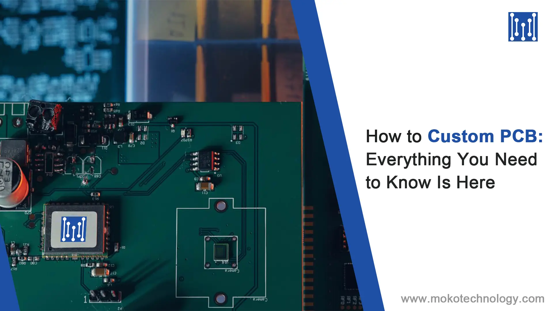
A custom PCB is a circuit board that is designed and manufactured according to exact specifications for a specific application, rather than using an off-the-shelf or standardized board. Met meer dan 90% of electronic devices using custom designed PCBs as their core component, it’s no wonder that custom PCB fabrication has become a critical service for supporting today’s complex and innovative electronic products. Whether you need a simple single-sided board or a multilayer beast with thousands of components, a custom PCB provides the perfect foundation.
This blog covers everything on custom PCBs. We’ll look at the pros and cons of going custom, the cost of custom PCB, and walk through the custom PCB fabrication process step-by-step.
Pros and Cons of Custom Circuit Board
Voordelen:
Tailored to Specific Needs: Custom circuit boards are designed to meet specific requirements, ensuring they are perfectly suited for a particular application.
Optimized Performance: Custom boards can be optimized for performance, leading to enhanced speed, efficiëntie, and overall functionality.
Space Efficiency: Custom designs can integrate multiple functions into a single board, saving space in the final product.
Cost Efficiency in Bulk: While initial setup costs can be high, custom boards can be cost-effective in large production runs due to reduced material waste and optimized manufacturing processes.
Improved Reliability: Custom boards can be engineered for specific environmental conditions, leading to increased reliability and durability.
Nadelen:
High Initial Costs: Designing and prototyping custom circuit boards can be expensive, especially for small production runs or individual projects.
Complexiteit: Custom designs require a deep understanding of electronics and may involve complex engineering challenges, requiring skilled professionals.
Time-Consuming: The design and testing phases of custom circuit boards can be time-consuming, leading to delays in product development timelines.
Limited Support: Off-the-shelf components often come with extensive documentation and support, which might be limited for custom-designed boards.
Lack of Standardization: Custom boards might not adhere to industry standards, making it challenging to find compatible components or troubleshoot issues.
How Much Does a Custom PCB Board Cost?
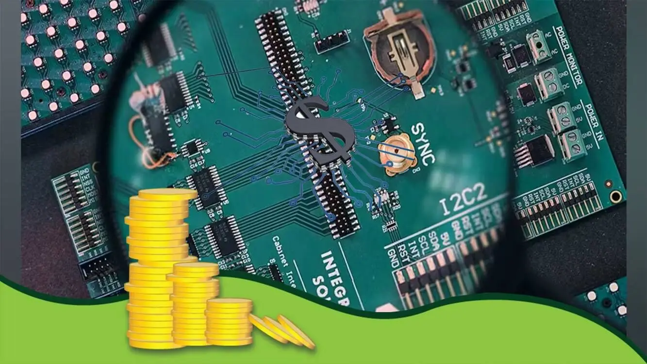
Custom PCB prices vary widely depending on design complexity, materialen, layer count, and manufacturing methods. More complex circuits, high-end materials, extra layers, and special processes like HDI all increase costs. Custom PCB costs often fall between $10-$50 for simple designs. More complex boards with advanced features can cost hundreds per unit. Manufacturing in bulk or placing larger orders generally leads to a reduction in the cost per unit. But the exact custom cost is decided by specific requirements, to know the actual price, you should consult PCB manufacturers and provide them with detailed specifications to get an accurate cost estimate for your custom PCB board, inclusief:
- The complete Gerber-bestanden
- Board Maat
- Aantal lagen
- Draai tijd
- Required quantities
- Materiaalvereiste:
- Einde vereisten
- Vereisten voor panelisatie
- Montagevereisten: (inclusief turnkey)
How to Custom PCB Boards-Step by Step
- Componentselectie en behoefteanalyse
The first step is to assess the intricate requirements of your PCB board. Dit omvat het kiezen van geschikte componenten zoals de voeding en processor. U moet een blauwdruk maken van al deze vereisten. Check out our other blog to get more knowledge about PCB components: Printplaatcomponenten: Een uitgebreide gids
- Design the PCB
De volgende, design the PCB layout with the help of custom PCB design software. De typische output van de software is een PCB schematisch Gerber-bestand, die informatie codeert zoals boortekening, volglagen, en componentannotatie, onder andere parameters:.
- DFM checking
The next step is to run a Design for Manufacture (DFM) controleer voordat u kunt beginnen met de fabricage van printplaten. Dit zorgt ervoor dat het ontwerp geen afwijkingen heeft.
- Print de binnenste lagen
Dit omvat snijden, schoonmaken, en het drogen van het epoxysubstraat voordat je de film die je in de laatste stap hebt gevormd op je paneel plaatst. Tenslotte, UV-behandel het paneel.
- Het ongewenste koper etsen
An alkaline solution is used to wash away any unhardened part of the copper layer, ervoor zorgen dat de vereiste koperlaag intact is.
- Het register ponsen voor uitlijning van lagen
This involves optically punching the different layers for registration hole creation and ensuring that there is alignment.
- Geautomatiseerde optische inspectie
In deze stap, je zult een lasersensor moeten gebruiken om de lagen te scannen terwijl je zoekt naar discrepanties tussen de Gerber-bestanden en de uitkomst.
- Laag op en hecht
Betreft het aan elkaar lijmen van de PCB-paneellagen met een aluminium persplaat.
- Boren
The next step is to drill holes into the PCB stack, allowing the electrical components’ placement and interconnection.
Further reading: PCB-boren: Alles wat u moet weten, vindt u hier
- Koperafzetting en platting
To cover the non-conductive materials and bond the panels, je moet het hele paneel bedekken met een nieuwe koperen laag.
- Beeldvorming van de buitenste laag en koperetsen
Involves applying a photoresist material over the outer copper layer and imaging it.
- Toepassing soldeermasker
Het bord wordt schoongemaakt voordat het soldeermasker wordt aangebracht, die het bord beschermt tegen kopercorrosie, schade, en oxidatie.
- Goud/zilver oppervlakteafwerking en zeefdruk
Ter bescherming van de koper- en soldeercomponenten op de pads, je moet de printplaat met goud of zilver plateren. Het volgende is om door te gaan met profilering of zeefdruk, wat inhoudt dat kritieke details op het bord worden afgedrukt, zoals de bedrijfsnaam, foutopsporingspunten, onderdeelnummers, en aangepaste PCB-fabrikant-ID.
- Elektrisch testen
Sondetesters worden gebruikt om open- en kortsluitingstests op uw bord uit te voeren, wat zorgt voor functionele betrouwbaarheid. Duurzaamheidstests volgen dit.
Our Capabilities and Services for Custom PCB Fabrication
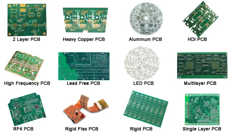
Manufacturing Different PCB Types
MOKO-technologie, as a leading custom PCB manufacturer, is able to fabricate a wide array of PCBs, inclusief:
- Hoogfrequente printplaat
- Zware koperen printplaat
- LED-printplaat
- RF4-printplaat
- Microware-printplaat
- Stijve print
- Koolstofinkt PCB
- Enkelzijdige printplaat
- Dubbelzijdige printplaat
- Meerlagige printplaat
- Halogeenvrije PCB
- Loodvrije PCB
- Standaard printplaat
- Aluminium printplaat
- HDI-printplaat
- Stijve-flex PCB
- Hoge TG-printplaat
Aangepaste PCB-oplossingen die wij aanbieden
- Prototype-PCB
We kunnen afronden 700 PCB-prototypes in minder dan een week voor uw test of presentatie. Met onze bijgewerkte hoogwaardige apparatuur en snelle fabricagemogelijkheden, we zijn meer dan zeker om in een mum van tijd aan uw eenvoudige of complexe PCB-prototypebehoeften te voldoen.
- Circuit Board Design
We bieden unieke ontwerpdiensten op maat om aan uw specificaties en toepassingen te voldoen via ons uitgebreide proces dat omvat:; voorlopig ontwerp, prototype ontwikkeling, productie integratie, en tenslotte, productie.
- Massaproductie van PCB's
MOKO’s PCB factory is equipped with advanced equipment and experienced operators, which allows us to complete customer orders within the fastest turnaround time, from small batches to large batches.
- PCB-assemblage
At our manufacturing facility, we utilize a range of advanced PCB assembly techniques to meet the unique requirements of each customer’s project, inclusief SMT, THT and Mixed PCB assembly, en BGA PCB-montage.
- ERP systeem
Ons ERP-systeem garandeert een kostenefficiënte productie van PCB's door middel van automatische planning, stabiele materiaaltoevoer, capaciteits planning, en realtime monitoring om de productiemogelijkheden te vergroten.
onze mogelijkheden
| Parameter | Omschrijving |
| Materiële basis | FR4, Halogeenvrij materiaal, Rogers HF-materiaal, Hoge TG FR4, CEM-3, |
| Aantal lagen | 2-36 lagen |
| maximale PCB-dikte: | 3.2 mm, bijzonder: 6.50 mm |
| Min PCB-dikte | 0.1 mm |
| Maximale bordgrootte in mm | 480 X 580, bijzonder: 584.2 X 1041.4 |
| Koperen krassen | 18 of 35 µm, M: 9 µm, 210 µm, helemaal tot max. 350 µm |
| Min spoorbreedte in MIL | 3/3 of 4/4 of 5/5 of 6/6 of 7/7 |
| Minimale gatdiameter | 0.2mm, 0.3m, enzovoort |
| Oppervlakteafwerking | Goud, Van mening zijn, HASL met en zonder lood, Zilver |
| dirigent volgt intervallen | 100 µm |
| Soldeer-stop-maskers | Verwijderbaar soldeermasker, een UV-geharde soldeerresist, en een droogfilmmasker |
| Ontwerpopties | Bond gebieden, SMD |
| Afdrukken markeren | Het kan in alle pakkende kleuren |
| Mechanische bewerking | krassen, molen |
| Andere afwerkingsopties | metallisatie van gaten met zilver, koolstofcoating |
MOKO-technologie- A Reliable Custom PCB Manufacturer
Hoogwaardige grondstoffen: ons strikte leveranciersselectiebeleid, gestandaardiseerd inkoopproces, en traceerbare bron van grondstoffen zorgen ervoor dat we kunnen werken met hoogwaardige grondstoffen.
Geavanceerde apparatuur: Our investments in advanced manufacturing tools streamline production and deliver exceptional quality. This equipment helps slash production lead times for a faster time to market and lower custom PCB costs.
Sterke productiecapaciteit: Met meerdere jaren ervaring en zware investeringen in de PCB-productie-industrie, ons bedrijf heeft zowel het ervaren personeel als de apparatuur om uw gewenste productiewerklast en kwaliteit te ondersteunen.
Uitstekende kwaliteitscontrole: Kwaliteit staat centraal in onze productie. Naast samenwerking met certificeringslaboratoria zoals UL, we hebben een strikt intern kwaliteitscontrolebeleid om ervoor te zorgen dat elke printplaat aan de norm voldoet;.
Snelle en stabiele levering: We doen er alles aan om u te helpen die strikte deadlines te halen via ons betrouwbare en gestroomlijnde leveringsproces.
24-uur ondersteuning: Productieproblemen of vragen kunnen zich op elk moment voordoen - onze betrouwbare 24-uurs ondersteuningsmedewerkers helpen u bij elk probleem dat u heeft.