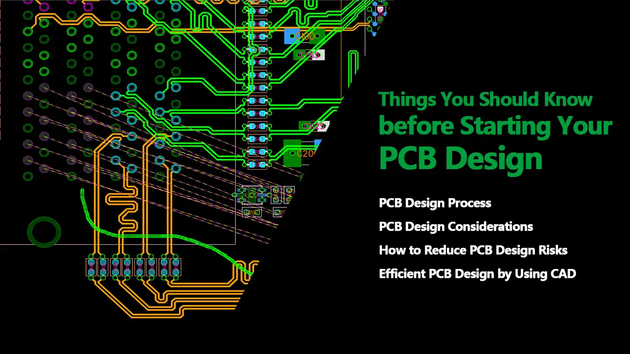
PCB Schematic: What Is It? Why Is It Important?
A printed circuit board design starts with a PCB schematic diagram. This PCB schematic layout visually depicts the electronic circuit as a graph, using symbols to represent components and lines to show their electrical connections. Typically, the PCB schematic is developed prior to the physical board layout. Once the circuit board schematic is verified to match the intended design and project specifications, work on the PCB layout and fabrication can proceed. A PCB schematic enables an engineer to comprehend how the various components interconnect and their particular functionalities. This knowledge is vital when repairing or reproducing a printed circuit board. The following guide explains the step-by-step process of designing PCB board schematics. Let’s read on.
How to Design a PCB Schematic?
Step 1: Set page size
Evaluate projected schematic size and complexity early when selecting page dimensions. Beyond standard A4, larger A3, and A2 sheets accommodate substantial circuits spanning hundreds of components across complex multi-page hierarchies. If containing a straightforward circuit, compact A5 or A6 pages may suffice.
Step 2: Name pages
Set up cover sheet listing page names/numbers for navigation. Employ intuitive grouping by allocating basic function-oriented names – “Power Supply”, “Microcontroller Configuration”, “Sensors Interface” etc. Alternatively, categorize by stages in data flow – “Inputs”, “Processing”, “Outputs”. Follow standard alphanumeric sequencing and avoid large gaps between page numbers for appends.
Step 3: Establishing grid guidelines
While not an immediate demand by the designers, setting up a grid serves as a necessary reference for the tool. A grid facilitates precise referencing of components and their connections. It ensures that circuit elements adhere to the grid, enabling seamless network probing during inspection.
Step 4: Page title bar
Situated at the bottom of the schematic page, the footer houses comprehensive details. It encompasses the page dimensions, board ratings, revision histories, circuit’s name/function, copyright marks, and so on.
Step 5: Add supporting notes
Designers are tasked with documenting essential circuit notes. These notes can be drafted on separate documents or on pages alongside the schematic drawings. Particularly for intricate designs, annotations are often detailed on separate pages, covering aspects like jumper states and PCB layout constraints.
Step 6: Track revision history
Tracking revisions involves documenting alterations made to the design. It includes dates of modifications, descriptions of changes, contributors’ and reviewers’ names, as well as review comments. This log typically resides on the primary or final page of the schematic layout.
Step 7: Schematic document directory
The directory serves as a catalog of topics within the schematic documentation. It significantly aids designers in locating specific modules within complex designs. For smaller and simpler designs, this step can be omitted if deemed unnecessary.
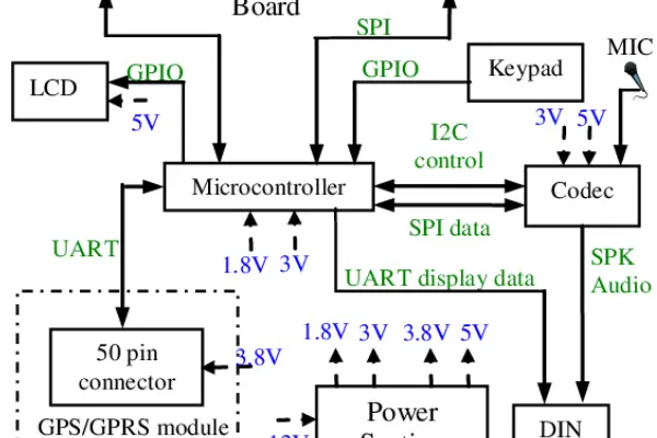
Step 8: Draw block diagram
Develop block diagram encompassing key modules – processors, memory units, peripherals, external interfaces and other principal sub-systems. Denote crucial connections and data flows at block abstraction level.
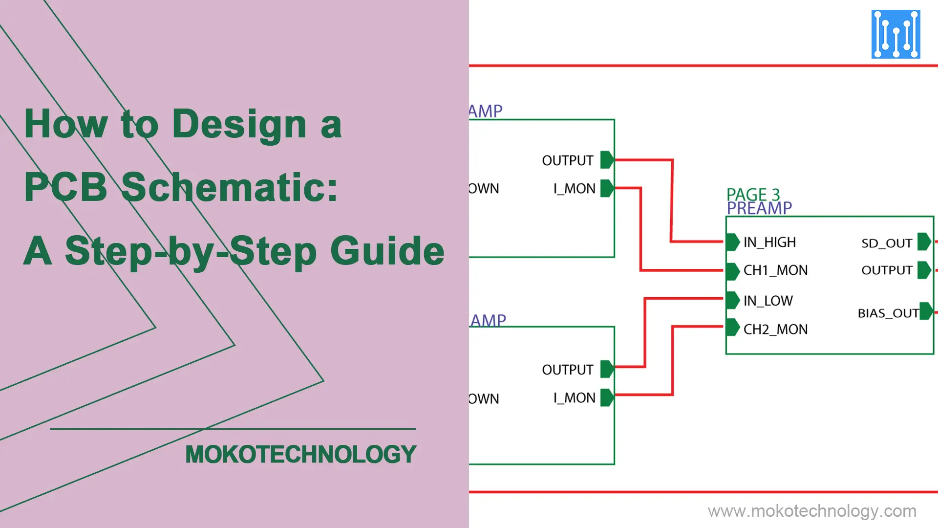
Step 9: Layered schematic diagram design
In cases where the PCB stackup is intricate with multiple modules, adopting a layered schematic structure proves most effective. This hierarchical depiction visually illustrates signal flow between modules. Clicking on a module provides an in-depth view of its details.
Step 10: Component reference
This reference table lists standard electronic components alongside their designated reference indicators used across schematic diagrams. Indicators adhere to IEEE criteria, emphasizing the use of uppercase letters for specific component naming.
| Component | Reference Designator | Component | Reference Designator |
| Resistor | R | Battery | BT |
| Capacitor | C | Cable/wire | W |
| IC (Integrated Circuit) | U/IC | Switch | SW |
| Diode/LED | D | Fiducial | FD |
| Fuse | F | Oscillator | OSC |
| Inductor/Bead | L | Plug /Connector | P/CON |
| Zener diode | Z | Heatsink | H |
Further reading- Circuit Board Components: A Comprehensive Guide
Step 11: Symbolic generation
Schematics encompass various elements like active, passive, and connectors, incorporating components such as transistors, diodes, logic gates, processor ICs, FPGAs, and operational amplifiers. Passive devices like capacitors, inductors, and transformers are included. While creating new components is discouraged unless absent from the standard library, adherence to IEEE standards for symbol creation is crucial.
Step 12: Operational amplifier configuration
Adhering to IEEE standards when creating symbols is vital, especially for operational amplifiers. Simplifying the drawing process, designers often follow standard configurations, placing input pins on the left and output pins on the right, with power and ground pins positioned vertically. Ensuring alignment with manufacturer datasheets is crucial when altering symbol orientation or connections.
Step 13: Heterogeneous schematic notation
Components like PGAF, memory units, and microprocessors, characterized by multiple pins (data, input/output, address, control, and power lines), necessitate distinct notation for each subcomponent within a single package to maintain clarity.
Step 14: Network connections
Clarity in circuit comprehension is achieved by appropriately marking intersection points where wires share electrical connections. Simplifying schematic diagrams involves representing integrated circuit (IC) common symbols instead of excessively drawing networks. Emphasizing organized pin-to-pin connections between devices with matching names enhances readability.
Step 15: Strategic component placement
Thoughtful placement of elements within the schematic significantly impacts subsequent bill of materials and IC package creation.
Step 16: Design rules checking
Utilizing Design Rule Checking (DRC) within CAD ensures both logical and physical integrity of the design, evaluating compliance with enabled design rules during planning.
Step 17: Net table verification
Post-schematic design completion, generating the netlist is crucial for layout import. This process produces machine-readable (.mnl) and human-readable (.txt) files displaying electrical connections. Manual verification of networks is advised to prevent design errors.
Step 18: Bill of material
Modern CAD tools offer a BOM creation feature, contingent on designers inputting all necessary data during part creation or import. The BOM comprises vital information like manufacturing part numbers (MPN), package details, supplier names, or supplier part numbers, essential for accurate documentation.
Step 19: Schematic list
Often overlooked but critical, the logical schematic list serves as a crucial organizational tool based on past design experiences. Checklists minimize errors in diagrams, ensuring error-free schematics that facilitate the layout designer’s work.
Conclusion
This guide presents a thorough summary of creating circuit board schematic. Whether starting out new to schematics or looking to get advanced knowledge, this comprehensive guide aims to be a valuable reference for creating high-quality, effective printed circuit board schematics through all stages from concept to finalization. Please contact us if you have any other queries.