PCB アセンブリは非常に複雑なプロセスです, そこでは常に正確さが重要です. 最も小さな欠陥でも、電子機器内で複数の問題が発生する可能性があります。. There are still a number of various defects that can negatively affect the functioning of PCBs and their application in electronics; one of the most widespread of them is the so-called “PCB tombstone” or “tombstoning. But do you know what is it? What should you do to avoid this issue? Let’s dive in to find the answer.
What is PCB Tombstone?
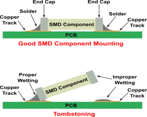
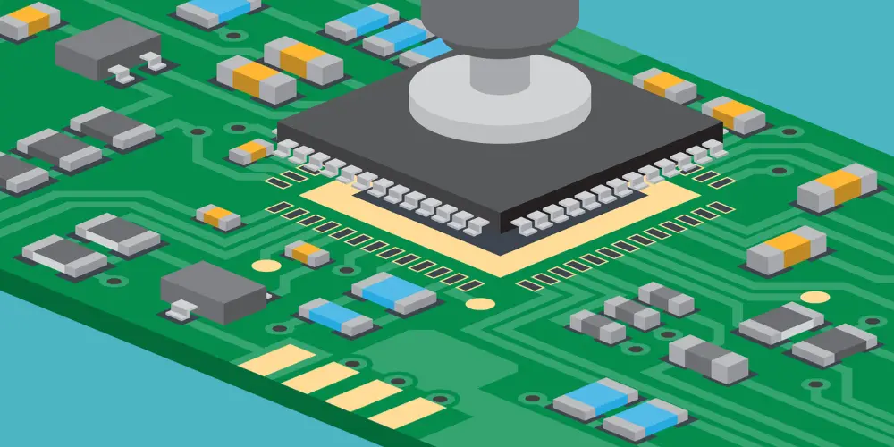
PCB tombstone is also commonly known as the Manhattan effect, Stonehenge effect, or drawbridge effect, which is a soldering defect that is likely to happen during the surface mount components assembly process. It’s termed this because an affected part looks like a tombstone in a graveyard in appearance. When tombstoning happens, one end of a surface-mount component (often a passive part such as a resistor, コンデンサ, 等) is kept lifted off the PCBパッド, while the other end remains in the soldered position. This problem usually occurs on some smaller SMT components. The smaller the size, the greater the risk.
7 Main Causes for PCB Tombstone
At its core, tombstoning itself is caused by an imbalance in the forces acting on the component during the soldering process. To understand this phenomenon, we need to explore the idea of “wetting” in the soldering process. Wetting refers to the process where molten solder forms a bond with the metal surfaces of both the component lead and the PCB pad. In an ideal scenario, wetting occurs simultaneously and uniformly on both ends of a component. しかしながら, when wetting is uneven, it can lead to tombstoning. Several factors can contribute to the imbalance that causes tombstoning:
-
Uneven thermal profiles
Temperature gradients within the PCB can make one end of a component to solder before the other end. This is caused by the inconsistent heat distribution in the reflow oven or the changes in the thermal characteristics of the PCB board materials.
-
Inconsistent solder paste application
When the amount of solder paste applied to the pad is inconsistent, it will cause uneven wetting. The reason for inconsistent solder paste amount is usually due to improper stencil design or improper solder paste printing process.
-
Pad design issues
If pad sizes are mismatched or the layouts of the pads are not right, then it is probable to develop different surface tension forces. Even with slight differences in pad dimensions, tombstoning is likely to occur especially when it is a case of small parts.
-
Component geometry
Some of the shapes and dimensions of components can be more inclined to tombstoning due to their physical characteristics. 例えば, components with asymmetrical designs or larger aspect ratios are usually more sensitive.
-
PCB material properties
Fluctuations in 熱伝導率 across the board are one of the main causes of irregular heating. This is especially true in the case of multi-layer boards which have irregular copper density in inner layers.
-
Surface finish variations
Some of the PCB finishes influence solder wetting. Conventional Hot Air Solder Leveling (HASL) finishes are cheaper; しかしながら, they cause surface imperfections that promote tombstoning.
-
Component placement issues
Misalignment of parts on the PCB would affect the soldering process, which will lead to high risks of PCB tombstone.
The Impact of PCB Tombstoning
While a tombstoned component might seem like a minor issue, its consequences can be severe and far-reaching. 最初, it would affect the function of the whole electronics. When tombstoning occurs, it leads to the formation of an open circuit which in turn leads to partial or in the worst of cases complete failure of the device. 2番目, even if a tombstoned component maintains some contact, it can lead to intermittent connections, resulting in unreliable performance over time. 最後, detecting and reworking PCB tombstone is not an easy job that will increase manufacturing costs and time.
How to Prevent the PCB Tombstone?
幸運にも, there are several strategies that PCB designers and manufacturers can employ to minimize the risk of tombstoning:
- Optimize pad design: Designing the pad with consistent sizes and making sure they have proper spacing to getgood wetting of the solder.
- Fine-tune the reflow profile: During the soldering process, it is important to control the heating and cooling rates to maintain thermal balance.
- Improve solder paste application: Use high-quality stencils andoptimize the printing process for uniform paste deposition.
- Consider component orientation: Have components on the reflow oven in a position that is along the moving direction of the board to ensure equal heating.
- Use appropriate PCB finishes: For those small SMT components that are prone to tombstoning, it would be better to choose finishes like ENIG, 浸漬スズ, or OSP that can provide more uniform surfaces.
参考文献: 8 一般的な PCB 表面仕上げ: 正しいものを選択する方法?
- Refine component placement:Make sure all components are assembled with high accuracy by utilizing advanced pick-and-place machines.
- Optimize PCB layout: In inner layers, focus on the copper distribution to make the heat distribution even. Thermal vias and balanced copper pours will help with the distribution of heat in your board.
結論
PCB tombstone is still a problem that plenty of electronics manufacturing companies encounter. With device miniaturization and high numbers of circuits, solutions to this problem are important. By understanding the causes of PCB tombstone and the corresponding measures, tombstoning incidences can be prevented or at least reduced greatly by the manufacturers.
MOKO Technology is one of China’s leading PCB companies, with almost two decades of experience in creating PCB assembly. Our expertise guarantees the highest quality and reliability in PCB assembly services. Do not let tombstone defects get in the way of your creativity and innovation. G私たちにご連絡ください to find out how we can assist in your project!