PCBバックドリリングとは? 使用する理由?

PCBの設計と製造には多くの課題があります, その 1 つは、信号の完全性と高速データ転送速度を確保することです。, にとって重要なものは 高周波基板. PCB バックドリルがこの問題を効果的に解決できることは言及する価値があります。. 記事上で, バックドリリング技術の徹底的な概要を提供することを目的としています。, その定義をカバーする, 利点, 段階的なプロセス, 等々. Let’s just dive right in…
PCBバックドリリングとは?
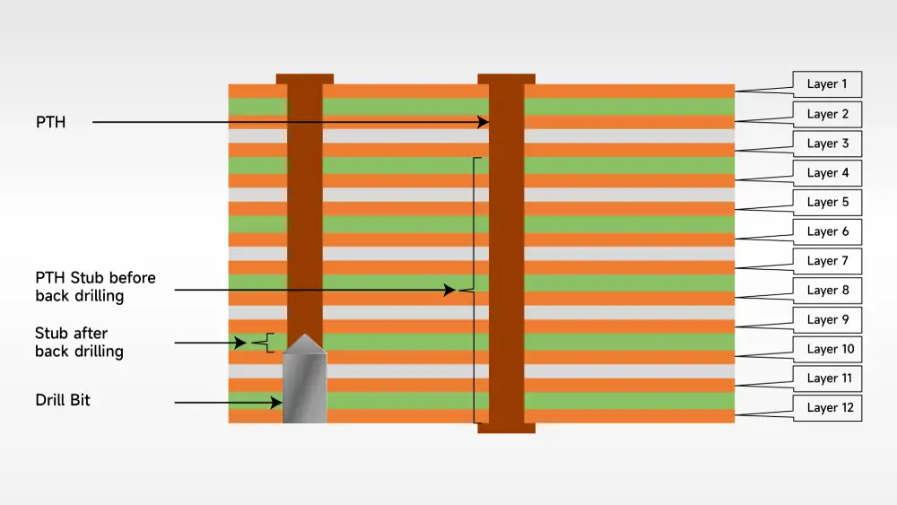
基板バックドリル加工工程, 制御深さ掘削とも呼ばれます, 多層 PCB のスタブを除去してビアを作成することが含まれます。. バックドリルの目的は、不要なスタブによる干渉なしに、基板の異なる層間の信号の流れを促進することです。.
When to Use Back Drilling?
It is generally recommended to consider adding the technique when the circuit track on the PCB board with a frequency range between 1GHz and 3GHz . しかしながら, 高速相互接続リンクの設計は複雑なシステムエンジニアリング作業です, チップの駆動能力や相互接続リンクの長さなどの他の要素も考慮する必要があります。. したがって, システム相互接続リンクのシミュレーションは、バックドリルが必要かどうかを判断する最も信頼できるアプローチです。.
PCB Back Drilling Example
バックドリル加工をわかりやすく説明するため, 例を考えてみましょう. があると仮定します 12-層PCB 1層目と12層目をつなぐスルーホールあり. 目的は、第 1 層と第 9 層のみを接続することです。, 10層目から12層目までは未接続のまま. しかしながら, the unconnected layers create “stubs” that can interfere with the signal path, シグナルインテグリティの問題が発生する. バックドリルでは、信号伝送を改善するために基板の裏側からこれらのスタブをドリルで開けます。.

Why Is Back Drilling Needed in PCB Fabrication?
- バックドリルにより信号の減衰を軽減します, より強力で信頼性の高い信号を確保する. さらに, この技術は、インピーダンス整合に対するスタブの影響を最小限に抑えるのに役立ちます。, これにより、EMI/EMC放射が減少します。.
- バックドリルは信号の歪みの問題を防ぐ効果的な方法でもあります. ビア スタブは確定的なジッターを引き起こすことでよく知られています, 信号のクロストークが原因で発生する可能性があります, EMI, そして騒音. これらのスタブを削除すると、, バックドリルは、確定的なジッターの原因を排除するのに役立ちます, 信号品質を改善し、信号歪みの問題を防止します.
- バックドリルによりビア間のクロストークを最小限に抑えることができます.
- バックドリルを導入することで, 信号内の確定的なジッターを軽減できます, 全体の減少につながる可能性があります ビット誤り率 (BER)信号の.
- 共振モードの励起の減少. 私
- 埋め込みビアやブラインドビアの使用を最小限に抑え、PCB 製造を簡素化します。.
- デザインとレイアウトへの影響を最小限に抑えます.
- 拡張されたチャネル帯域幅;
- 逐次積層に比べて低コストが実現可能.
How Back Drilling Works?

がある 5 key steps involved during the PCB back drilling process, below is a detailed breakdown of each step:
ステップ 1: Initial Drilling
最初, drill a plated through-holes (PTH) to create electrical connection among different layers of the board. Then plate the hole with copper to achieve conductivity between the required layers.
ステップ 2: Identification of Via Stubs
Analyze the PCB design and determine whether vias contain a stub that is not needed. Such subs would affect the signal integrity and cause the signal degradation.
ステップ 3: Back Drilling Setup
Before start the back drilling, it’s critical to setup a CNC drilling machine to ensure precise control. さらに, the selection of drill bit also matters. It should slightly larger than the hole diameter, usually 0.1-0.2mm.
ステップ 4: Back Drilling Process
このステップでは, PCB would be fixed into the CNC machine firmly, and the machine drills from the opposite side of the board. This process can remove the excess stub portion of the via without damaging the surrounding structure.
ステップ 5: Cleaning and Inspection
Once the back drilling is done, the PCB should be cleaned to remove residual debris, such as drill chips or copper particles. 最後に, check the back-drilled holes to verify if they are drilled with correct depth and diameter.
上 6 PCB バックドリリングの設計ヒント
- 適切なバックドリリングを確保するには, バックドリル層を含む個別の出力ファイルを PCB ボードの製造元に提供する必要があります。, どの層に対応するバックドリルが必要かを詳述した仕様とともに.
- バックドリル穴の直径は、最初のドリル穴の直径より少なくとも 0.2 mm 大きくする必要があります。, 層を通るバックドリルとトレースの間の距離は、最初のドリルで 0.35 mm、バックドリルで 0.2 mm である必要があります。.
- PCB スタックアップ設計時, 穴あけすべきではないトレースへの穴あけを避けるために、誘電体の厚さを考慮する必要があります。. 特定のレイヤーにドリルが必要な場合 (such as layer “L”), the dielectric thickness between the adjacent layers that do not require drilling and layer “L” should be at least 0.2mm.
- To optimize the back drilling process, ビア スタブの数を最小限に抑え、ブラインド ビアを避けることが重要です.
- それほど重要ではない領域にビアを配置し、バックドリル穴と信号トレース間の最小距離を維持することも、信号の反射やその他の問題を防ぐのに役立ちます。.
- バックボードの穴の横のトレースやプレーンの損傷を避けるために、バック ドリルの穴の直径を小さく保つことが重要です。.
課題 バックドリル加工の様子
- バックドリル深さ制御
ブラインドビアを正確に加工するには、バックドリルの深さの制御が不可欠です. バックドリル深さの公差は主にバックドリル装置の精度と中厚公差に影響されます。. しかしながら, ドリルの抵抗などの外部要因, ドリル先端角度, カバーボードと測定ユニット間の接触効果, 基板の反りもバックドリルの精度に影響を与える可能性があります. 生産中, 最良の結果を達成し、バックドリリングの精度を制御するには、適切なドリリング材料と方法を選択することが重要です。. バックドリルの深さを慎重にコントロールすることで、, 設計者は高品質の信号伝送を確保し、信号の完全性の問題を防ぐことができます。. - バックドリル精度管理
バックドリリングの正確な管理は、後工程のプリント基板の品質管理にとって非常に重要です。. バックドリルには、一次ドリルの穴径に基づいた二次穴あけが含まれます。, 二次穴あけの精度が重要です. いくつかの要因, 基板の伸縮含む, 装置の精度, および穴あけ方法, 二次穴あけ一致の精度に影響を与える可能性があります. したがって, バックドリルプロセスを正確に制御してエラーを最小限に抑え、最適な信号伝送と完全性を確保することが重要です.
結論
PCB 信号の完全性を確保するための重要な方法として, バックドリルは広く使用されています PCB製造工程. このブログを読んだ後、このテクノロジーをよりよく理解し、使用できるようになることを願っています. 他にご質問がある場合は, あなたはできる コンタクト 私たち 弊社の専門家にご相談ください. 中国の大手PCBメーカーとして, MOKO Technology はすべての PCB を備えています eあなたを助けるために必要な専門知識とスキル.


最近の投稿
インピーダンス整合: A Critical Factor in High-Speed PCB Design
Impedance matching has become a cornerstone of the signal integrity in the realm of high speed PCB…
How to Clean a Circuit Board Safely and Effectively?
It is important to learn how to clean a circuit board properly if you’re working…
Counterbore vs Countersink: Which to Choose for Your PCB?
When designing PCBs, selecting the appropriate type of holes for fasteners is crucial. And much…
PCB Copper Foil: 種類, プロパティ & 選び方
PCB copper foil is one of the most critical materials in the printed circuit board…
MOKO Technology Launches Vietnam Manufacturing Base in February 2025
深セン, 中国 - 2月 11, 2025 - MOKOテクノロジー, a leading global electronics manufacturing service…
PCB Solder Mask: What It Is and Why Every Circuit Board Needs It?
While most people focus on the components and copper traces that make up PCBs, there's…