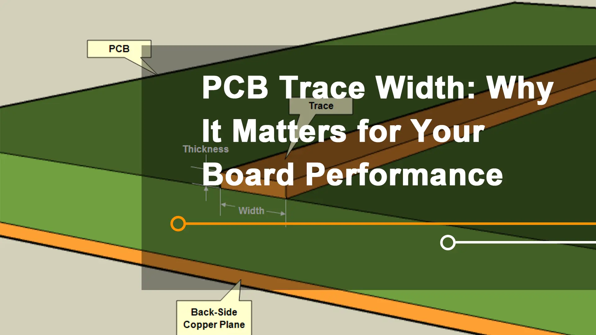
If you mean the copper thickness of the copper layer, there is actually no standard thickness, 0.5オズ, 1オズ, 2オズ, 3oz or other copper thicknesses are available. It mainly depends on the requirements of your product;
続きを読む: 重い銅のPCB
#PCB設計

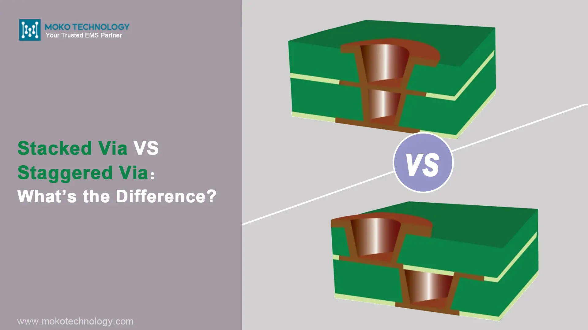
高度なエレクトロニクス用の複雑なプリント基板を設計する際の一般的な質問は、層間の接続の配線にスタック ビアを使用するか、スタッガード ビアを使用するかということです。.