As technology continues to advance in the electronics industry, packaging remains one of the key success factors determining efficiency and reliability. One example of such technology that received considerable attention in the last few years is the Ball Grid Array (BGA). 確かに, this innovation in packaging has significantly altered the interconnection of components to these printed circuit boards to enable high density and high performance. Here in this guide, we will cover over a brief overview of the BGA technology that includes its benefits and downsides, different types of BGA packages, BGAはんだ付け, and Ball Grid Array inspection techniques. すぐに飛び込みましょう.
BGAとは( ボール・グリッド・アレイ ) PCB上で?
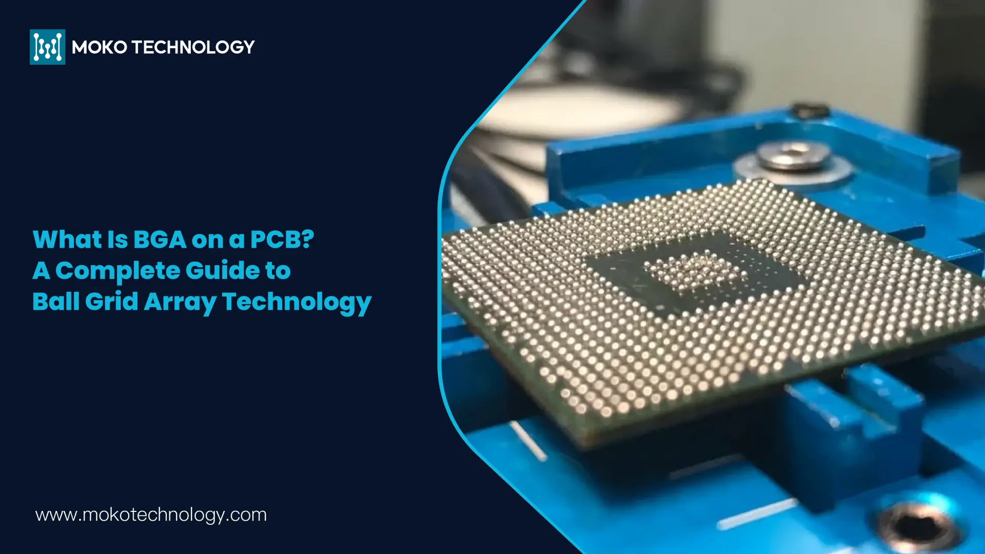
A Ball Grid Array is actually a type of surface mount packaging used in the manufacturing of 集積回路. Unlike other packages which utilize leads extending from the periphery of the package, BGA uses a grid pattern of solder balls at the underside of the package. These solder balls used as the contact points between the chip and the printed circuit board.
6 Commonly Used BGA Package Types
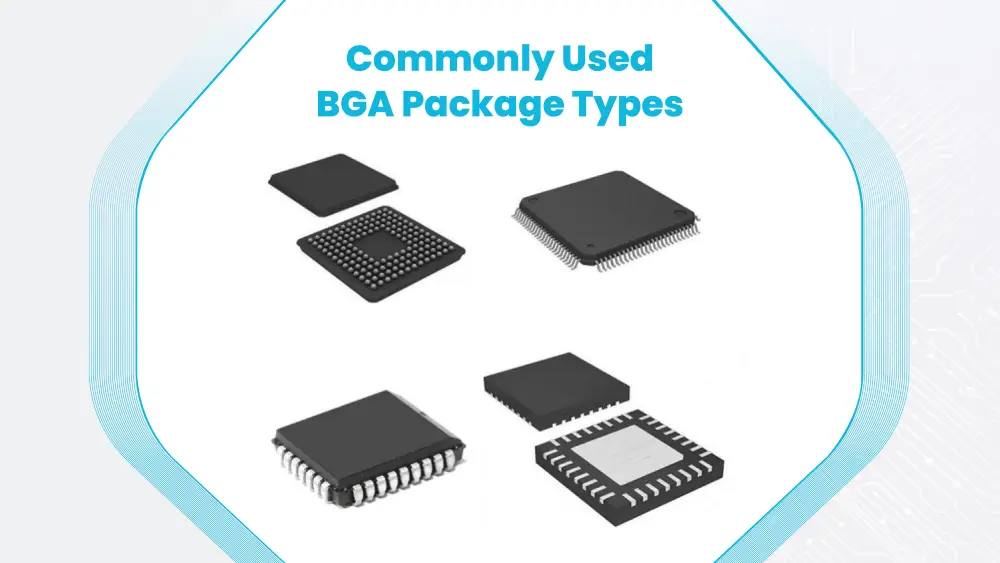
In the market, there are various types of BGA packages used for different applications and requirements. ここに, we will discuss six commonly used BGA package types:
-
PBGA(プラスチックボールグリッドアレイ)
In PBGA, the substrate is BT resin/glass laminate, while the packaging material is plastic.The feature of this type of BGA package is that it does not require additional solder to connect the solder balls into the desired package. It is an affordable solution for a number of applications.
-
セラミックBGA (CBGA)
CBGA is a kind of traditional ball grid array packaging type, which uses multilayer ceramic substrate as the base material. The metal lid is then soldered to the substrate using packaging solder to shield the chip, leads as well as the solder balls. The solder ball of it is mad from eutectic solder material, providing reliable connections between the substrate and the components.
-
マイクロ BGA (uBGA)
マイクロ BGA (µBGA) is an advanced Ball Grid Array packaging technology that takes up very little space. It offers much smaller chips; enhanced thermal management and increased density of data. As the name suggest, µBGA is primarily used in compact electronic devices and brings the much-needed enhanced performance in areas of size limitations.
-
テープBGA (TBGA)
テープボールグリッドアレイ (TBGA) is the kind of BGA packaging technique which uses the flexible tape instead of the rigid laminate. This can provide for light-weight and thin packaging with high density interconnects along with better thermal/ electrical characteristics.
-
Flip Chip Ball Grid Array (FC-BGA)
In FC-BGA, the integrated circuit is flipped so that it can be soldered onto the circuit board. This type of BGA package offers improved thermal and electrical performance as its solder balls connect to the PCBパッド 直接.
-
パッケージ上のパッケージ (ポップ)
In this kind of BGA package, many integrated circuits are stacked together. Each IC has its own ball grid array to enable components integration in a vertical way. It is widely used for applications that space is limited such as mobile devices.
| タイプ | 材料 | Solder Type | 主な機能 | 一般的なアプリケーション |
| PBGA | plastic | Leaded or lead-free | No additional solder needed for ball-to-package | 家電, low to mid-range applications |
| CBGA | セラミック | 共晶 | Long-standing type, protective lid | High-reliability applications, 航空宇宙, 軍隊 |
| uBGA | プラスチック | Not specified | 小さいサイズ, better heat dissipation | High-frequency operations, compact electronic devices |
| TBGA | プラスチック | Not specified | Thinner, ライター, high-density interconnections | Portable electronics, スマートフォン, タブレット |
| FC-BGA | Various | Direct to PCB | Enhanced thermal and electrical performance | High-performance processors, GPU, network processors |
| ポップ | Various | Multiple BGAs | Vertical integration, 省スペース | モバイルデバイス, where space is premium, memory+processor stacks |
Advantages and Disadvantages of BGA Technology
利点
- Higher Density: Compared with traditional packages, BGAs allows more components be connected even in a small space, which is crucial for modern electronic devices.
- Improved Thermal Performance: The solder balls are arranged in a particular pattern, making them uniformly share heat, thus reducing the risk of overheating in some areas
- Reduced Inductance: In BGA, the shorter connect paths can minimize inductance, so as to enhance the signal integrity, which is particularly helpful at high frequencies.
- Better Reliability: When comparing with the leaded package, BGA provides greater reliability as there are fewer mechanical stresses it should bear during the thermal cycling process.
短所
- Inspection Challenges: It’s more difficult to inspect the quality of BGA’s solder joints as they are located at the underside of the package. Some soldering issues are hard to check only by naked eyes. We have to use specialized techniques like X線検査.
- Repair Complexity: One of the downsides of BGA technique is the repair complexity. It is a time-consuming and costly process that requires professional tools such as BGA rework station.
- Highly Cautious Assembly: During the BGA soldering process, operators must be very careful to mount the components correctly, any mistake can affect the performance and even lead to poor connection.
How to Solder Ball Grid Array to Circuit Boards?
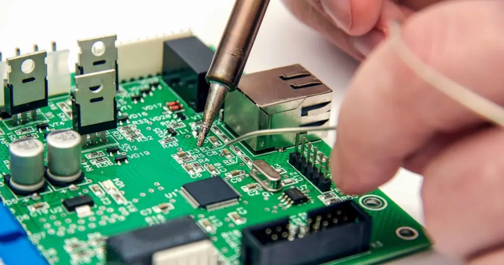
There are several key steps when soldering BGA packages. 最初, we need to clean the PCB board and apply solder flux to the PCB pads. 2番目, place the package in the desired areas of the board accurately. その後, the board with the mounted BGA components will undergo リフローはんだ付け, where the flux and solder balls would be melted, and when it is cooling, there is a solid connection between the ball grid array and the board. 最後, we need to conduct BGA inspection to check if there are any soldering issues such as bridges or voids. If any issues are found, we need to repair them by using specialized BGA rework equipment.
Ball Grid Array Inspection Techniques
- 電気試験
In electrical testing, we need to use specialized equipment such as multimeter and flying probe tester to ascertains parameters including resistance and continuity within BGA components. It discovers problems in connection performance and checks if solder joints are operating correctly.
- X線検査
By using x-ray inspection, we can check the internal structure of BGA without damaging the package. It allows us to identify solder joint issues and some hidden problems such as insufficient solder or voiding.
- Visual or Optical Inspection
The process of visually inspecting includes using magnification tools to look at BGA components and identifies surface troubles, such as misalignment and bridging. The assessment is fast, yet it only covers visible problems.
BGA Capabilities at MOKO Technology
MOKO Technology is proud of our sophisticated BGA assembly and inspection techniques. We use advanced facilities and modern technology, which enable us to guarantees both precision and quality at every assembly phase, enabling us to handle almost all BGA packages. Our collection of BGA services includes custom BGA assembly, highly advanced inspection techniques, engineering support, and rapid prototyping. If you require one-stop BGA PCB assembly services, do not hesitate to reach out to us.