La crescente domanda di elettronica avanzata guida le innovazioni nelle capacità e nelle prestazioni dei circuiti stampati. I progettisti di circuiti ora lavorano abitualmente con velocità di segnale più elevate. Segnali ad alta velocità, una volta una sfida occasionale, are becoming standard in printed circuit board layouts. Flawless transmission of high-speed signals requires designers to understand best practices for routing traces on boards. Traces can no longer be routed based solely on aesthetics or cost. The priority now is creating optimal trace paths to ensure signal integrity and minimize performance issues. To accomplish this, designers must grasp the knowledge of PCB transmission line. In questo blog, we will introduce the types of transmission lines used, discuss their importance, and provide preferred layout methods.
What Is PCB Transmission Line?
A printed circuit board transmission line transports signals between transmitters and receivers on a circuit board. It consists of two conductors – a signal trace and a return path, typically a ground plane. The conductors are separated by a dielectric layer. High frequency alternating currents exhibit wave propagation on transmission lines. A key property is that at each point along its length, the line has an impedance. inoltre, if line dimensions do not vary, this impedance remains uniform. Such a trace is termed a controlled impedance transmission line. Non-uniform impedances lead to signal reflections and distortion. Thus for high frequencies, controlling trace impedance predicts signal behavior.
Types of PCB Transmission Lines
When designing printed circuit boards, engineers have three primary options to consider for transmitting signals across the board:
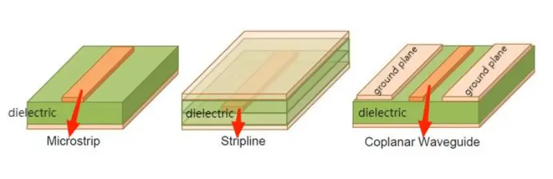
- PCB Microstrip
The microstrip transmission line consists of a single conductive trace acting as the signal carrier, routed over a reference ground plane. This reference plane, typically situated on one of the outer layers of the Impilamento PCB, provides the return path directly beneath the signal trace. Microstrips most commonly run along the exterior layers due to ease of access, tuttavia, it is also possible to embed these traces within inner board layers. The reference plane for an internal microstrip is still located on an adjacent outer layer. Microstrips enable simple routing for single-ended signals, high trace density designs, and suitability for surface mount components.
- PCB Stripline
Stripline transmission lines involve enclosing a routed conductive trace between two reference ground planes, contained within the board dielectric layers. This setup provides return current paths both above and below the signal carrier. The added shielding from two planes gives striplines natural immunity to electromagnetic interference compared to microstrip lines. Striplines exhibit excellent versatility – traces can be positioned closer to one reference plane or another to tweak performance, and multiple traces can be routed in parallel between the planes. The larger reference planes also promote superior signal transmission quality. Striplines do come with more complex fabrication versus microstrips, but enable excellent high-speed signal.
- Coplanar Transmission Lines
The coplanar transmission line places the signal trace and return paths on the same PCB layer. It consists of a central signal trace flanked by two wider ground planes, with spacing gaps separating the conductors. All coplanar elements route over the board’s dielectric material. Precise control of the gaps between trace, piani terrestri, and plane widths is imperative to achieve target impedances. Coplanar lines see less frequent usage compared to microstrips or striplines, but provide some advantages like easier impedance adjustment and not necessitating drilling vias. Their exposure also eases probing for measurements. But coplanars come with tighter fabrication tolerances and remain prone to EMI without shielding planes.
The Importance of Transmission Lines in PCB
As electronic devices and circuits push to faster switching speeds and higher frequencies, accounting for transmission line effects in PCB layouts becomes critical. At microwave frequencies reaching gigahertz ranges, traces can no longer be treated simply as connections between points. Piuttosto, the laws of electrical propagation dictate signals will reflect and ring based on the impedance of the trace geometry. Failure to control these effects results in distorted signals, interferenza elettromagnetica, and unreliable circuit operation. By properly implementing transmission lines—with controlled dimensions and spacings to achieve target characteristic impedances—PCB designers can perfectly transfer signals from source to load. Expertise with transmission lines, whether microstrip, stripline, or coplanar constructions, helps prevent signal degradation while enabling cutting-edge technologies. With today’s trends of miniaturization and constantly rising frequencies, an understanding of PCB transmission lines serves as a fundamental skill for designing high-speed, high-frequency circuit boards.
Tips When Designing Transmission Line

Controlling characteristic impedance along the entire trace length is paramount for transmission lines. Failing to do so results in disruptive signal reflections at high frequencies, corrupting data transmission. By tailoring line widths to achieve target impedances, designers create precision interconnections. Online calculators, CAD tools with integrated calculators, or seeking guidance from PCB manufacturers simplifies achieving accurate impedance targets, which standards like IPC-2581 also facilitate.
With impedance-controlled traces established, additional design practices optimize layouts:
Avoid Congested Areas – Prevent impedance discontinuities by routing lines away from tight spaces. Splits or breaks in traces disturb the return current path.
Use One Layer – Minimize vertical transitions using primarily one layer for easier impedance control and reference plane access.
Add Vias – If transferring between layers is unavoidable, place vias alongside traces as ground references maintaining the return path.
Keep Pairs Together – Route differential pairs together on the same path to match line lengths, avoiding obstacles like vias that may skew signals.
In sostanza, controlled-impedance transmission lines require meticulous planning and layout to deliver pristine signals at high frequencies. Myriad resources exist to accurately design trace geometries and spacings for target impedances prior to routing. After calculation, care must be taken to implement lines with consistency and continuity. With today’s signal speeds entering microwave ranges, expertise using impedance-matched transmission line principles marks an invaluable PCB design skillset. Mastering controlled-impedance traces and mitigating discontinuities enables reliably routing high-frequency signals.
Avvolgendo
In chiusura, comprehending transmission line fundamentals empowers printed circuit designers. Impedance control along entire trace lengths is paramount; discontinuities disrupt signal integrity. By computing physical dimensions for target impedances, uniform interconnections reliably transmit high-speed data.
Please reach out with any outstanding questions on this crucial PCB layout topic. Whether addressing impedance calculations, transmission line configurations, routing methods, or signal integrity concerns, we eagerly support your pursuit of expertise.