Anche i più piccoli difetti nell'assemblaggio di un circuito stampato (PCBA) può comportare grossi problemi in futuro per i produttori di elettronica. Schede difettose che superano i test e arrivano ai clienti’ le mani rischiano fallimenti sul campo, riparazioni costose, e danni duraturi alla reputazione del tuo marchio. So how can you catch these minute defects before they become headaches? The answer is automated optical inspection (AOI) – an extremely useful quality control technique designed specifically for inspecting PCBAs during production.
But what exactly is AOI and how does implementing it lead to higher quality finished boards? In questo blog, I’ll give an overview of how AOI technology works and why implementing it can drastically improve your inspection process. Alla fine, you’ll see why AOI should be a core part of your quality management strategy.
What Is Automated Optical Inspection?
Automated optical inspection is an automated quality control method used in electronics manufacturing that visually inspects printed circuit boards and assemblies for defects during production using computer vision cameras and software. AOI provides fast, coerente, and detailed inspection by capturing high resolution images to check for flaws like missing components, wrong parts, poor solder joints, and other issues, without physical contact with the boards. Implementing AOI enables early detection of defects before value is added, leading to improved quality, higher yields, and reduced manufacturing costs.
https://www.www.youtube.com/watch?v=ncBWtigSu3w
How Does Automated Optical Inspection Work?
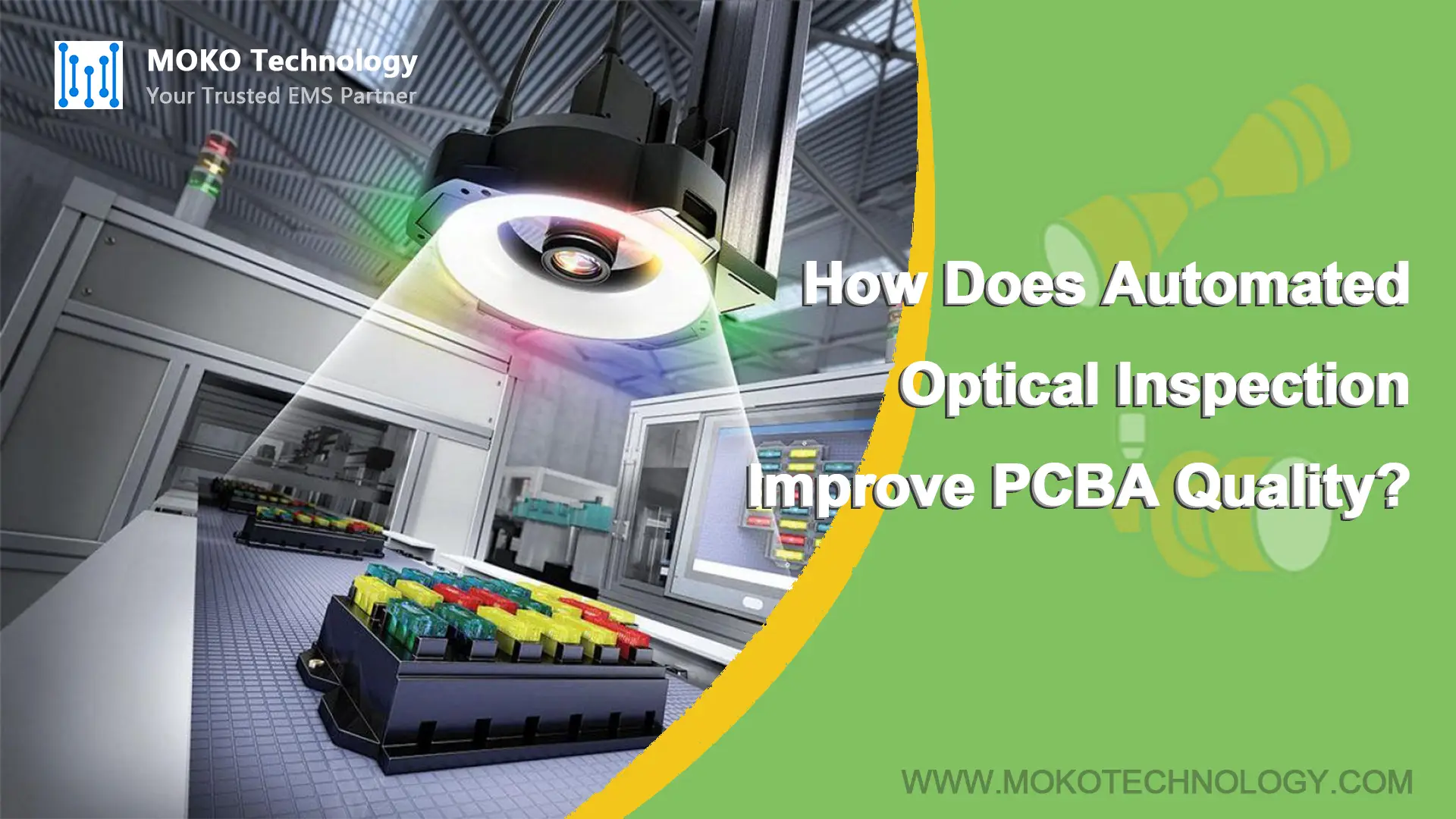
An AOI machine uses multiple light sources to illuminate a PCB from different angles, along with high-resolution computer vision cameras or video cameras to capture comprehensive images of the board. The PCB moves along a conveyor under the cameras. Precision transport mechanisms and advanced lighting ensure clear images highlighting components, solder joints, markings, and other features across the entire board surface. AOI software then analyzes the captured images, scanning them autonomously to check for defects without the need for human visual inspection. The algorithms compare images to a golden board reference, inspecting for defects based on programmed standards. Any problems found are flagged and classified by type, with images and data recorded.
Benefits of Automated Optical Inspection
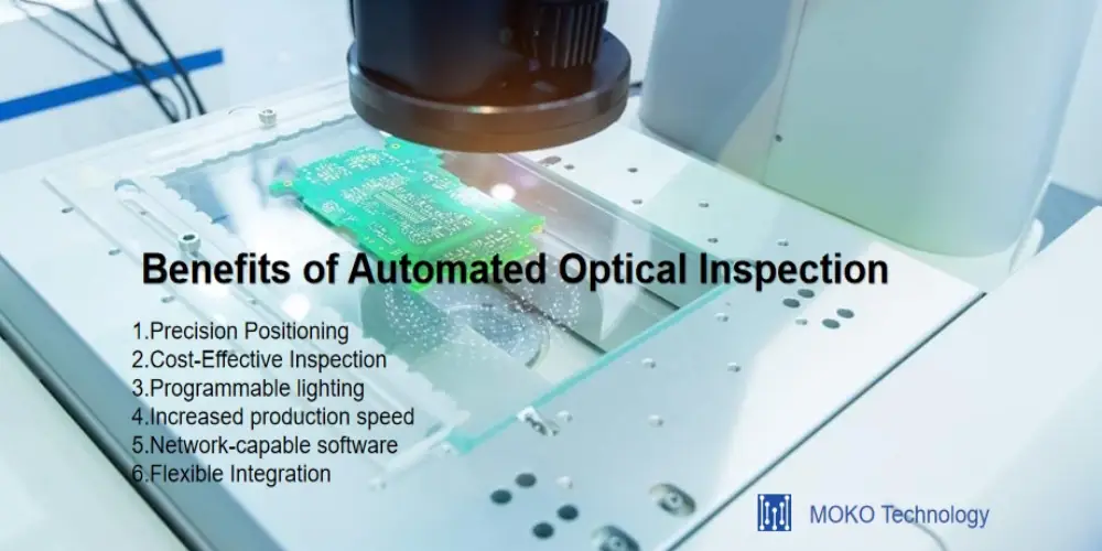
- Precision Positioning
The precision of the positioning in production equipment and AOI machines is a critical factor. Even minute deviations in placement can result in many flaws. Automated optical inspection offers superior accuracy in detecting small positional inconsistencies.
- Cost-Effective Inspection
AOI provides rapid, repeatable and affordable inspection. The installation process is straightforward with online guides, enabling quick deployment. AOI testing can improve pass rates for PCBs, lowering overall costs.
- Programmable lighting
Proper lighting is key for machine vision applications. The electronics field is constantly evolving, so no single light source can reveal every potential defect. AOI systems can configure arrays of lights in software and optimize contrast to uncover different flaws.
- Increased production speed
Automated inspection is much faster than manual inspection. AOI systems can operate 24/7 and inspect parts at high speeds. This increases throughput and productivity.
- Network-capable software
AOI utilizes advanced network-capable software tools to enable zero-defect manufacturing. AOI provides flexible solutions for any PCB inspection need. Data collection and access are critical AOI capabilities. It can gather information in various formats like images, text and more.
- Flexible Integration
AOI offers excellent flexibility, allowing deployment at any production stage. Performing AOI post reflow soldering is often best, as major defects tend to occur after soldering.
Defects That PCB Optical Inspection Can Find
AOI is capable of detecting a wide range of defects on the surface, dimensions, componenti, and PCB itself.
- For surface defects, AOI can identify issues like nodules, graffi, ammaccature, coating errors, e altro ancora. It uses imaging techniques to analyze the entire surface, finding any irregularities that may impact performance or longevity. Even tiny defects invisible to the human eye can be detected.
- When inspecting dimensions, AOI checks for problems like open circuits, corto circuiti, thinner solder, and violations of spacing or width guidelines. Precise measurements on solder joints, Tracce di PCB, and other features quickly identify any out-of-spec dimensions. This helps avoid functionality issues or mechanical weaknesses.
- Inspecting components, AOI can find wrong, missing, or misaligned parts. It confirms component presence, orientamento, skew, and polarity against PCB design files. Flipped, compensare, or tombstoned components are easily flagged. AOI also inspects solder joints, paste coverage, and more to ensure proper attachment.
- For the PCB itself, AOI checks for short circuits, excess copper, missing pads, spacing violations, and via issues. It can detect any damage, breakage, or errors in mounting components. This comprehensive inspection protects circuit integrity and performance.
AOI Test from MOKO Technology
Alla tecnologia MOKO, we utilize automated optical inspection as one key process to deliver high-quality printed circuit boards to our customers. Our AOI systems use advanced cameras and image processing software to efficiently identify assembly errors and defects. This technology improves detection accuracy over manual visual inspection, especially for complex PCBs and high-volume production.
In addition to AOI, we employ a range of other testing methods to verify PCBA quality, Compreso test con sonda volante, automatic X-ray inspection, prove in circuito, PCB electrical testing, e così via. For more information about the AOI test, please click here to send us a message, and we will promptly respond with more details about our capabilities.
