Is there a standard that defines that the marking actually has to indicate the cathode?

SMD LEDs normally have some kind of marking. We recently had 300 PCBs manufactured where each had 32 LEDs of those. However, the assembly house placed all LEDs in reverse. The cathode is not consistent with the marking of the actual LED that was mounted. Is there a standard defining this?

No. It is entirely up to the component manufacturer. When the PCB is manufactured, some companies will ask that component placement overlays be given. Designators are provided. And polarity marks for all polarized components are shown.

It’s also a good idea to make a couple of test boards and hand solder and get familiar with the components to identify this kind of issue, prior to sending in large batches to get assembled.

#PCB Assembly #PCB Testing
Picture of Oliver Smith

Oliver Smith

Oliver is an experienced electronics engineer skilled in PCB design, analog circuits, embedded systems, and prototyping. His deep knowledge spans schematic capture, firmware coding, simulation, layout, testing, and troubleshooting. Oliver excels at taking projects from concept to mass production using his electrical design talents and mechanical aptitude.

What Others Are Asking

How much larger should a plated-through hole be than lead diameter to get good solder wetting?

I’m designing a new PCB where I have a whack of connectors that have to line up with the metalwork. There are some problematic connectors. All 4 pins are round. I want to have the holes as small as possible while allowing for good solder adhesion over the full length of the pin. I’m looking for guidance on how much clearance around the component lead I should have in order to get good solder wetting and adhesion.

Can I leave a through hole pad off one side of a machine-fabricated PCB?

I’m designing a two-layer PCB and I’m very inexperienced. A third-party company will fabricate them. Now, I have a PTH part with a number of closely spaced pins. However, I can’t greatly simplify routing by running traces unless I eliminate the pads for certain pins on one side of the board. So can I leave a through hole pad off one side of a machine-fabricated PCB?

Read Detailed Advice From Blog Articles

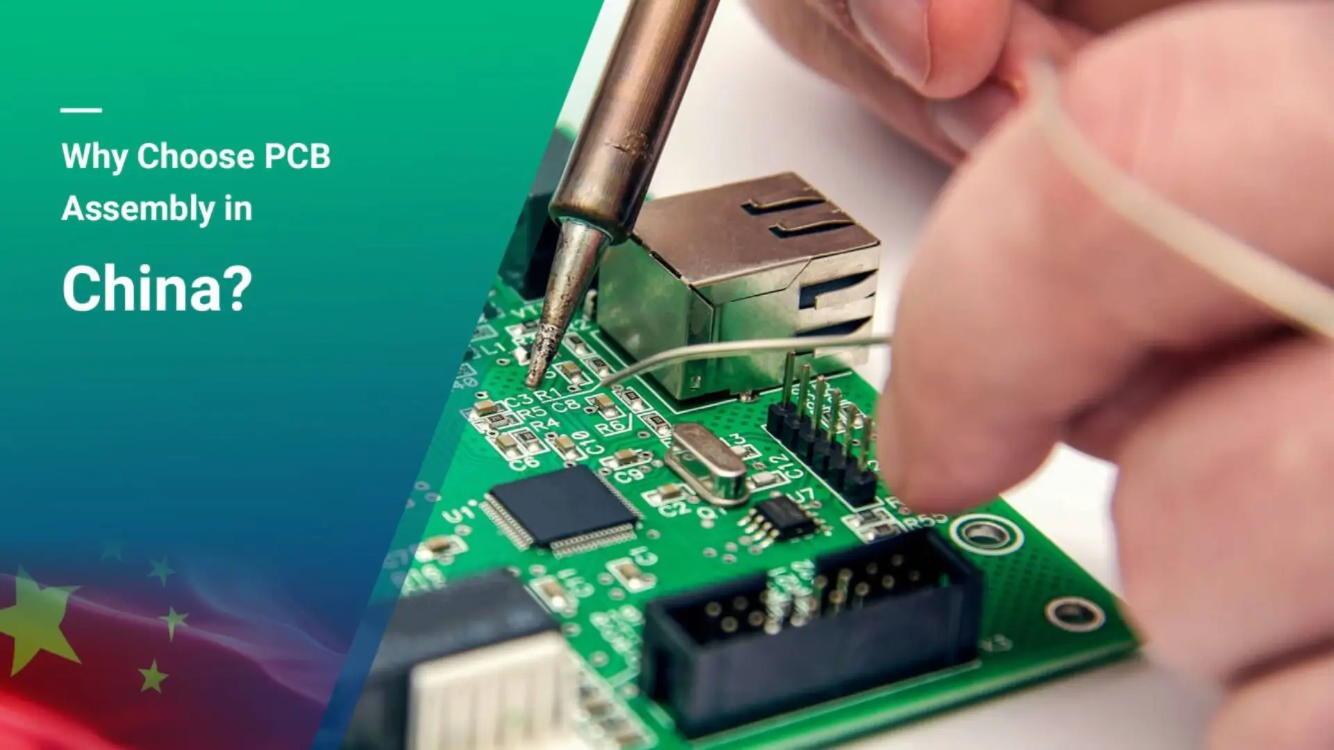
Why Choose PCB Assembly in China
Will Li

Why Choose PCB Assembly in China?

Printed circuit board (PCB) assembly is an essential step in electronics manufacturing. It involves soldering and assembling electronic components onto a bare PCB board to create a functional

Scroll to Top