Introduction to SMT PCB Assembly


SMT PCB assembly has become the most popular PCB assembly technology since the 1980s, and is now widely used in industries such as consumer electronics, healthcare, automotive electronics, and telecommunications. So, how much do you know about it? Like what is it? Why is it widely used? Well, read on, then you can find out in this blog.
What Is SMT PCB Assembly?


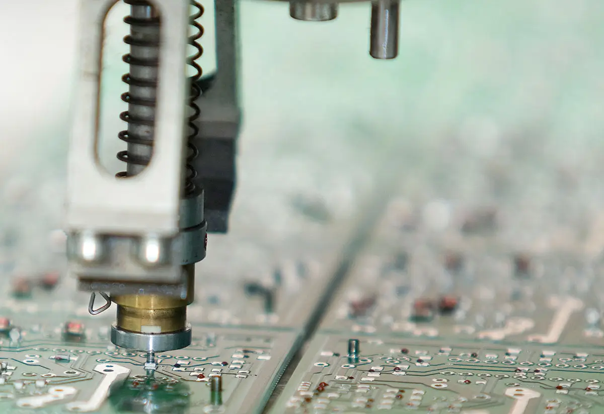
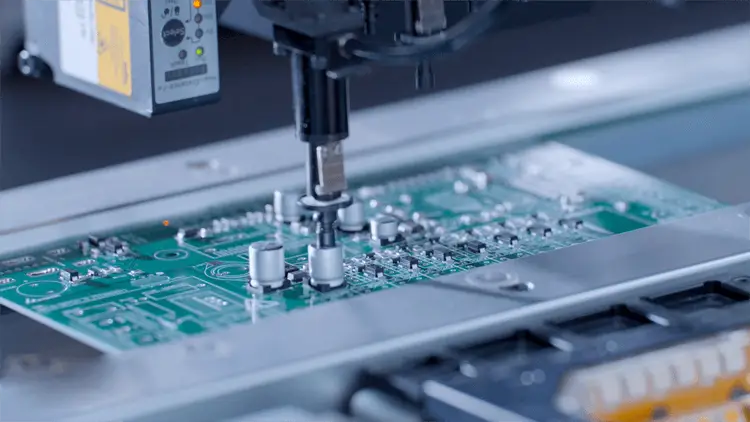
SMT PCB assembly refers to the process of assembling electronic components directly on the surface of circuit boards by using molten solder paste instead of inserting wire leads into drilled holes in the printed circuit boards. Currently, it is a process widely used for low-cost and high-volume consumer electronic assemblies. This technology is the best choice when the boards are required to accommodate a high density of components or when the space is limited. In addition, when mass production using automated technology is required, SMT PCB assembly is also recommended.
The Advantages of SMT PCB Assembly


- Lower Board and Material Cost
On the one hand, compared with THT, SMT PCB requires fewer drilling holes, which can greatly reduce the processing cost. And the smaller size of the SMT PCB reduces the overall bill of materials because there is no need to make room for holes. On the other hand, SMD components cost less than through-hole components in most cases, and the smaller size of surface mount components can also reduce handling, packaging, and shipping costs.
- High Production Efficiency
SMT PCB assembly is a highly automated process that not only reduces the possibility of errors but also significantly increases the production efficiency. For example, for the same quantity, it takes about half an hour to assemble components using SMT, while it might take several hours to complete the assembly using THT. Therefore, it can help manufacturers to improve their productivity.
- PCB Miniaturization
As people prefer to use portable electronics, PCBs tend to be designed to be smaller in size and lighter. SMT PCB assembly can minimize the size of the circuit board. Compared with through-hole components, the size and volume of SMT components can be reduced by 60%~70%, and the weight can be reduced by 60%~90%.
- High Signal Transmission and High Frequency
The high density of SMT PCB assembly can achieve high speed signal transmission as the short circuit and short delay. At the same time, SMT assembly can reduce the RF interference as SMD components have no leads or short leads.
The Disadvantages of SMT Assembly
We should realize that SMT also has some disadvantages, and this technology is not suitable for all assembly projects. Let’s discuss it one by one:
- Expensive Equipment
SMT PCB assembly line requires a large investment as the equipment involved costs much including reflow oven, pick and place machine, solder paste screen printer, and so on. For some start-ups, this is a lot of overhead and must be supported by a large number of orders in order to break even and make a profit.
- Prone to Damage
SMD components are more prone to damage when they meet physical shocks, they are also sensitive to ESD, so it is necessary to perform ESD protection during the assembly process and packaging.
- Hard to Inspection
It’s not easy to do inspection work as there are so many solder joints on the circuit boards and the size of SMD components is so small. Especially when it comes to BGA assembly, the solder balls and joints are even more difficult to inspect as they are under the components.
SMT Assembly Services at MOKO
Working with a qualified and reliable partner keeps your SMT PCB assembly going smoothly. MOKO Technology, as a top-notch PCB assembly service provider, offers clients turnkey assembly services from designing to after-market services and everything in between.
In the designing phase, our engineers would provide the best SMT assembly solution based on your project requirements by drawing on their expertise and rich experience. And our flexible assembly capacities allow us to deliver PCBAs with a quick turnaround time, we are capable to produce 10 million chips per day in the case of 5 SMT lines. We are capable of handling SMT prototypes, and low-volume to high-volume PCB assembly by using both manual and automated SMT assembly processes. We utilize cutting-edge equipment to perform single and double-sided placement of all component types.
More importantly, we care much about quality. We perform different testing methods to guarantee the high quality of each PCBA including visual inspection, automated optical inspection, X-ray inspection, and functional testing. If you are looking for a trusted PCB assembly partner, look no further, we are your best choice, contact us today to start your project!
Recent Posts
Impedance Matching: A Critical Factor in High-Speed PCB Design
Impedance matching has become a cornerstone of the signal integrity in the realm of high speed PCB…
How to Clean a Circuit Board Safely and Effectively?
It is important to learn how to clean a circuit board properly if you’re working…
Counterbore vs Countersink: Which to Choose for Your PCB?
When designing PCBs, selecting the appropriate type of holes for fasteners is crucial. And much…
PCB Copper Foil: Types, Properties & How to Choose
PCB copper foil is one of the most critical materials in the printed circuit board…
MOKO Technology Launches Vietnam Manufacturing Base in February 2025
Shenzhen, China - February 11, 2025 - MOKO Technology, a leading global electronics manufacturing service…
PCB Solder Mask: What It Is and Why Every Circuit Board Needs It?
While most people focus on the components and copper traces that make up PCBs, there's…


