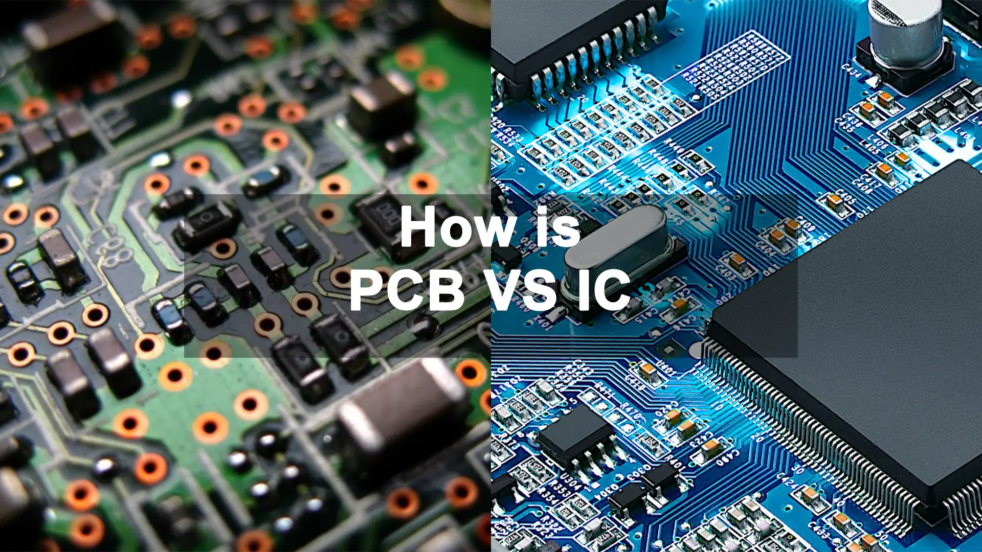
When you step into the electrical industry, IC and PCB must be two common words in your daily work. They sound similar but exactly different if you keep patient to look into them.
Induct You into the Comparison Between IC Vs. PCB
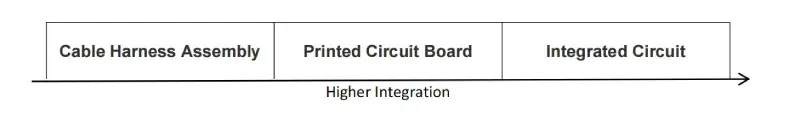
If we regard a rural house as cable harness assembly, PCB is just like a suite that contains a living room, bedroom, kitchen, bathroom, and balcony. It takes up only tens of square meters, but with complete configuration to serve human habitation as the big rural house.
Thus, the definition of PCB, printed circuit board, becomes easy to understand. Printed circuit boards are not only an important carrier of electronic components but also a provider of electrical connections of electronic components. It is named after its manufacturing method- printing. Specifically, a board ready for assembly should go through inner layer drilling, tracing, etching, black oxidation, lamination, outer layer drilling, PTH, PTRS, soldering mask, gold plating, HASL, silk legend, and testing.
Compared to PCB, IC is, properly, like a skyscraper or tall building, which embraces store floor, officer floor, canteen floor, and underground parking. It is highly integrated in layout.
For IC layout, it is all about function isolation and effective connection. For, example, artificial circuits and digit circuits is isolated. The power line and ground line are separated. And, sensing circuit is located at a corner far away from control logic system. There are a few layers that are in various layouts and construction. For instance, folding transistor is used for saving space and gate resistance in low-noise circuits. There is even H-shape design for a layer. Besides, elevators to different destinations are equipped so as to accelerate transmission. High-speed wires are used for connection between CPU and memory.
Know Clear About Different Manufacture Methods Between IC Vs. PCB

IC Manufacture
IC manufacture is about interconnecting the all the required wires and component, such as transistors, resistors, and capacitors on a small or several small pieces of semiconductor chips, and then packaging them into a miniature shell. It functions as partial circuit structure.
In particular, there are many package types. We are going to talk some common packaging as follows.
- DIP package (Dual in-line package) : This package is used in integrated circuits in early age. Its pins are led from both sides of the package, in the a vertical or double-vertical arrangement.
- PLCC package (Plastic led chip carrier) : This package is square in shape, with pins on all sides. It is much smaller than the DIP package. With the advantages of small size and high reliability, PLCC package is suitable for PCB surface mount technology..
- SOP package (Small profile package) : This package is for PCB surface mount technology. The pin is in both sides of the main body, shaping in L-form. Thanks to compact pin spacing, SOP packages are suitable for small and high density PCB.
- PQFP package (plastic square flat package) : This package is thin and flat. The pins surrounding the package are in L-shape or T-shape. PQFP package fits HDI mini PCB with good heat dissipation.
- BQFP package (four-side pin flat package with cushion) : This package is evolved from QFP package. The four corners of its body are cushioned against deformation and bending pin during transportation.
- QFN package (four-side pin-less flat package) : This package is configured with electrode contacts on four sides. With no pin, mount area it takes up is smaller than QFP, while the height is lower than QFP. However, the electrode contact does worse in burdening weigh, so sufficient protection should be applied during long-distance shipment.
- BGA package (ball grid array package) : One side of this package is attached with a spherical convex ball in an array arrangement. It is well known as good electric heat-sink, less signal transmission delay and high reliability.
In addition to the above common packaging methods, there are other useful packages methods for particular requirement, such as TO type packaging and MCM type packaging.
PCB Assembly
After finishing the printing process mentioned in Part One, we are going to getting PCB assembled by components. The PCB assembly technique contains through-hole assembly, surface mount assembly and the mixture.
- Through hole assembly: As its name, leads of the component is inserted through the hole drilled out of the PCB and then welded on the other side. This technique has been widely used for decades and is known for its stable connections. However, through-hole components generally require more space on the PCB, making them unsuitable to high-density PCB layout. Therefore, through-hole assembly PCBA is commonly found in old electronics, power electronics, and device that needs strong mechanical connections.
- Surface mount assembly: With surface mount technique, components are allowed to be padded directly on the board and welded to the trace through reflow soldering process. Besides, components for SMT is so small that they can be mounted on both sides of the PCB. Therefore, this technique are preferred when assembling high density PCB and compact electrical device. Nowadays, surface mount assembly have been a key technique in the market since it is space-saving and good at electrical performance.
- Mixture: Combination of through-hole and SMT is also an important solution for some special order in assembly house. In other words, there are both through hole and surface mount components on the final PCB. This flexible solution paves a way for those complex PCB and properly meets the demand of final market.
Understand the Applications of IC and PCB
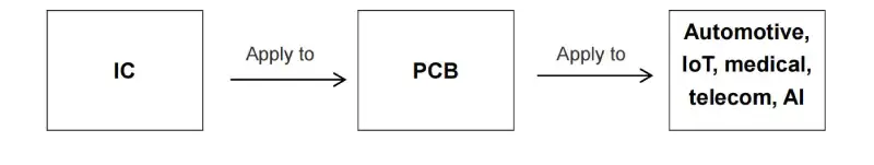
As a functional circuit, IC can be directly applied on PCB, improving compact features and reliability of the PCB. Then, PCB with IC is used in many high-tech industry, such as smart automotive, IoT, smart medtech, telecom and artificial intelligence.
Takeaway
All in all, PCB with IC is the basis of modern technology. It is widely used in many field and play an important part in society development