
Printed circuit boards (PCBs) are at the heart of electronics manufacturing. However, PCBs can sometimes experience failures due to a defect called delamination. PCB Delamination occurs when the layers of a PCB separate, leading to malfunction or failure of electronic devices. Addressing this problem can be costly and time-consuming. In this comprehensive guide, we will delve into the causes of PCB delamination, explore effective prevention methods, and discuss the best practices for PCB delamination repair.
What Is PCB Delamination?
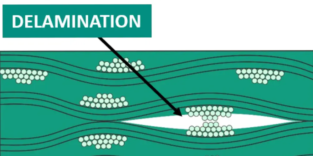
Delamination is an intralaminar separation between the laminated layers of fiberglass and resin that make up a multilayer PCB. It can range from minor splitting to complete detachment across large areas. This separation disrupts electrical connectivity and the function of a PCB. Cracks fracture the thin copper traces between layers, interrupting circuits. Further delamination can also lead to short circuits between layers once insulated.
Delamination primarily affects complex, multilayer PCBs rather than single or double layer boards which lack an interlaminar bond. If left unaddressed, delamination damage can expand rapidly, reducing operational lifespan and leading to ultimate PCB failure.

Causes of PCB Delamination
Delamination can stem from a variety of sources, including both manufacturing defects and operational stresses in the field. Understanding the root causes is key to preventing future occurrences. Common factors that contribute to PCB delamination include:
- Thermal Stress
Repeated heating and cooling leads to differences in thermal expansion and contraction between PCB layers. These mismatches generate mechanical stresses over time. Slow temperature changes during power cycling as well as rapid, localized heating can cause delamination.
- Mechanical Stress
Physical flexing of the PCB, shocks, and vibrations also introduce stresses between layers. Constraints on the PCB like mounts, fasteners, or chassis integration can concentrate stresses in certain areas.
- Lamination Process Defects
Insufficient bonding, uneven resin flow, contamination and voids between layers can create weak points prone to delamination. This demonstrates the importance of closely controlling lamination press parameters.
- Excessive Moisture
One of the most frequent causes of PCB delamination is moisture. Even a small amount of moisture that becomes trapped in the board can lead to cracking when the PCB is subjected to high temperatures, as the moisture turns to steam and expands. In many cases, poor bonding or inadequate adhesive between the layers of the board enables moisture to seep in.
- Excessive Bend Radii
Thin, flexible PCBs subjected to tight bends repeatedly experience focused interlayer stresses. Using adequate bend radii standards helps mitigate this. Now that we understand common delamination causes, let’s discuss ways PCB manufacturers and product designers can avoid these issues…
How to Prevent Delamination?
With knowledge of typical root causes, steps can be taken to minimize the risks of delamination in PCB designs and manufacturing:
- Material Selection
Research bonding films with maximum adhesive strength across full operating temperature range of end product, including thermal shock resistance. Ensure resin materials between layers have low coefficients of thermal expansion to match that of copper traces, reducing expansion mismatch strains. Require suppliers to provide lot testing data and certifications for resin quality, Tg, modulus, and elongation parameters.
- Moisture Control
Raw materials should be kept in storage rooms with desiccants to actively absorb humidity before use. Boards can be pre-baked prior to soldering to drive out any residual moisture. The assembly floor itself needs environmental controls like dehumidifiers to maintain optimal low moisture levels. Minimizing the time materials are exposed to ambient humidity is also important.
- Avoid Overheating
Overheating during the soldering process can lead to thermal stress, which in turn can cause delamination. Use appropriate soldering techniques, such as reflow soldering, and ensure that the temperature profiles are within the recommended range for both the components and the PCB.
- Process Controls
Closely control lamination heating/cooling rates, temperature dwell times, bonding pressure profiles, and resin flow parameters. Verify laminate quality through microsection analysis and bond strength destructive testing after pressing.
- Protective Coatings
Specify conformal coatings with high chemical, humidity, and temperature resistance to protect PCBs. Ensure complete coating coverage on all exposed surfaces to fully isolate from environmental ingress.
- Bend Radii Standards
Based on flex testing data, define and mandate minimum bend radii for PCB handling and installation to avoid overstress. Incorporate radius limits into assembly work instructions and quality inspection criteria.
The Best Practice for PCB Delamination Repair
If delamination is detected, specialized repair processes can detach, reinforce, and re-laminate layers to restore PCB integrity. Here is an overview of professional repair procedures:
- Remove conformal coating if present to access entire board.
- Use x-ray imaging to identify all areas of separation. Target only delaminated sections for repair.
- Carefully detach laminated layers using gentle heat and slicing technology to access damaged interface.
- Clean and prepare bonding surfaces. Reinforce with adhesive interlayer films featuring high peel strength.
- Use thermal compression bonding to re-laminate layers with optimal temperature and pressure.
- Inspect repair under x-ray and confirm restored mechanical and electrical integrity.
- Apply new conformal coating across entire board if needed.
Final Thoughts
Preventing delamination through robust PCB design and manufacturing is essential for product reliability. However, unforeseen factors can still lead to interlayer separation over time.
Incorporating strategies like simulation, testing, material selection, process control, and protective coatings reduces risks greatly. When delamination does occur, professional repair can often restore PCB functionality.
With the knowledge provided in this guide, you are now equipped to catch and address any PCB delamination issues with full confidence. Leveraging prevention best practices and repair techniques will lead to maximized electronics reliability and lifespans.


Recent Posts
Impedance Matching: A Critical Factor in High-Speed PCB Design
Impedance matching has become a cornerstone of the signal integrity in the realm of high speed PCB…
How to Clean a Circuit Board Safely and Effectively?
It is important to learn how to clean a circuit board properly if you’re working…
Counterbore vs Countersink: Which to Choose for Your PCB?
When designing PCBs, selecting the appropriate type of holes for fasteners is crucial. And much…
PCB Copper Foil: Types, Properties & How to Choose
PCB copper foil is one of the most critical materials in the printed circuit board…
MOKO Technology Launches Vietnam Manufacturing Base in February 2025
Shenzhen, China - February 11, 2025 - MOKO Technology, a leading global electronics manufacturing service…
PCB Solder Mask: What It Is and Why Every Circuit Board Needs It?
While most people focus on the components and copper traces that make up PCBs, there's…