Bringing your electronic ideas to life begins with PCB drawing, which is the process of converting your circuit design into a layout that can be used to create real boards. To the beginners or the person who wants to improve his skills, this guide will take you through all the significant steps in how to draw a PCB.
Step 1: Start with a Schematic
Drawing a PCB layout starts with a good schematic. The schematic is actually a diagram to illustrate how all the components in your circuit are wired or interconnected electrically. It can also be interpreted as the layout map of your PCB drawing.
Use Schematic Capture Software: Start with creating your schematic using PCB design software such as Altium Designer, Eagle, or KiCad. These are the tools that let you sketch out your circuit, place the components, and connect them properly.
Double-Check Connections: Make sure all the connections in your schematic are correct. Any mistakes here will be reflected in your PCB drawing and this may lead to a non-functional board.
Further reading: How to Design a PCB Schematic?
Step 2: Define the Board Outline
Once you have your schematic ready, the next task that you need to perform is to establish the sort of boundary for your PCB. In this step, we need to determine the size and shape of the board.
Set Board Dimensions: Define the shape and the size of your PCB according to the space that is normally available in the final product. Now in your design software, use the mechanical layer, and sketch the board outline.
Consider Mounting and Enclosure: Also ensure to consider thru-holes for stand-off and connectors as well as other features that should be accommodated in the box. The board outline should incorporate all these features so as to avoid some of these challenges during the construction.
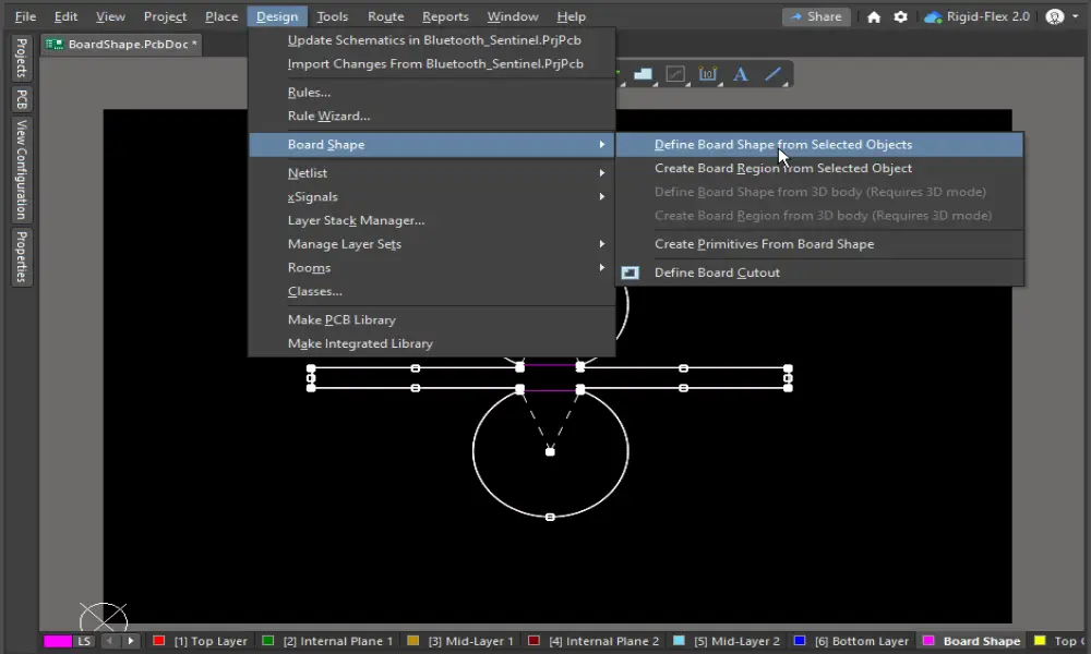
Image from Altium
Step 3: Place the Components
Now that the board outline is established, it is time to put components on the PCB. This step is always considered important because the orientation of components seriously affects the functionality and manufacturability of the board.
Import Components from the Schematic: Most of the PCB design software gives you an option of conducting an auto transfer of the components from the schematic to the PCB layout. This can make sure that all components are positioned and labeled correctly.
Strategic Placement: Place components based on the flow of the circuit, which is also crucial. For example, place connectors near the edges of the board, and try to put power components close to each other. While for sensitive components, we should put them away from high-noise areas.
Optimize for Routing: Organize components to achieve short and simple paths between components. This can avoid problems such as crosstalk and makes the signals more reliable.
Step 4: Route the Traces
Routing the traces is a critical step in circuit board drawing, which deals with the connection of the parts of your PCB with copper traces. We need to handle this step very carefully since it will greatly determine the electrical performance of the boards.
Route Power & Ground Trace: Generally we first do power & ground routing. For those PCBs that need to handle high currents, wider traces are necessary.
Signal Trace Routing: Routing the signal traces is up next. They should be routed as short and direct as possible in order to reduce both resistance and inductance.
Use Vias Properly: There are instances where two or more layers of the circuit board have traces that need linking, this can only be achieved by use of vias. Although they are required, they have to be applied in the right way. Too many vias can add a new sort of resistance and make the manufacturing process more intricate.
Follow Design Rules: PCB designers must follow the design rules provided by manufacturers which may include the minimum width of the conductive traces, the space between them, and the size of the vias.
Step 5: Add Labels and Silkscreen
The silkscreen layer is where you find the text, symbols, and labels that you want etched on the PCBs. This layer gives important data in the assembling and in the solving of mistakes. In this step,
Label Components: Make sure to print the reference designator of every component on the PCB (however small the text is, it is suggested to make it clear and easy to read, for example, R1, C1, and so forth). This helps when assembling the parts in that one sees a particular label of the part and knows where it belongs.
Add Polarity Markings: Regarding components like diodes, capacitors, and LEDs, add polarity signs that show the correct side of a component.
Note: Keep silkscreen markings away from pads and traces to prevent them from being covered by solder or causing interference.
Step 6: Perform a Design Rule Check (DRC)
Before finalizing your printed circuit board drawing, run the Design Rule Check (DRC) in your PCB design tool. The DRC checks your layout against the manufacturing requirements and notifies where traces overlay over each other, where clearances are inadequate, or where there are unconnected pins.
In addition to the automated check, perform a manual inspection to check if there are any issues missed. Pay particular attention to areas like power and ground planes.
Step 7: Generate Gerber Files
After you have your PCB drawing done and you are thoroughly checked for errors, the next step taken is to develop Gerber files. Gerber files are used in the industry as the recommended file type to produce PCBs by manufacturers. They consist of all the data necessary for the generation of copper layer files, silkscreen, solder mask, and drill files.
Layer-Specific Files: Create a Gerber file for each layer of your PCB: top and bottom copper, silkscreen, solder mask, and outline.
Drill File: As always, do not forget to create an Excellon drill file that is used to drill the holes for vias, pads, and mounting locations.
Review Before Sending: Once you have completed your work and before forwarding the files to your manufacturer, you must check all the files in a Gerber viewer to see whether you have produced what you intended.
FAQs about PCB Drawing
To draw a circuit board, what software should I use?
Some popular PCB design software includes Altium Designer, Eagle, and KiCad, each of which has different features. For example, KiCad is free and easy to use, while Altium Designer is preferred by professionals for its advanced features.
To help you choose a suitable PCB design software, read: 8 Leading PCB Design Software: A Comprehensive Comparison.
When drawing a circuit board, how do I determine the correct trace width for my PCB?
It depends on the current that traces need to carry and the acceptable voltage drop. To determine the appropriate trace width, you can also use online calculators.
How can I ensure that my PCB design will be manufacturable?
Ensure manufacturability by adhering to the rules and guidelines set by the manufacturer, and by arranging the components and employing as few vias as possible. In addition, make a prototype of your design to identify mistakes if any.
How do I avoid signal integrity issues in my PCB drawing?
To minimize signal integrity problems, PCB designers should keep the traces as short as they can be, and avoid sharp corners in your trace routing. Meanwhile, proper use of grounding techniques is also important. For high-speed signals, consider the usage of ground planes and controlled impedance traces.
Further reading: Mastering PCB Signal Integrity: Key Factors, Design Tips, and Testing Methods
What’s the best way to route power in a PCB design?
For power routing, use wider traces or polygon to handle higher currents. In multi-layer boards, it may be useful to employ separate power planes for different voltages. Make power trace runs short and use decoupling capacitors near the Integrated Circuits.