In recent times, there has been a growing trend towards miniaturization and increased intelligence in electronic products. This has resulted in designers utilizing smaller PCB boards to accommodate these design requirements, made possible through the use of High-Density Interconnect (HDI) PCB technology. HDI PCBs employ techniques such as blind vias, buried vias, micro vias, vias in pads, and very thin traces to accommodate more components in a smaller footprint while maintaining quality and performance.
And HDI PCB design is a critical process that necessitates expertise, experience, and the proper utilization of technology. In order to aid in your understanding of HDI layout and facilitate successful HDI PCB design, we are sharing some key considerations and suggestions to keep in mind during the design process in this blog, with the hope of inspiring you to create innovative HDI designs.
What Is HDI Layout?
HDI PCB design is a specialized approach that optimizes component placement on a printed circuit board (PCB) to maximize space utilization and minimize signal interference. It is particularly beneficial for designing compact and high-performance electronic devices like smartphones, tablets, and wearables.
There are various types of HDI layouts, including the sequential build-up, stacked vias, and microvias. In the sequential build-up, layers of the PCB are built up sequentially to achieve the desired density. Stacked vias involve drilling holes through multiple layers of the board to create interconnections. On the other hand, microvias are similar to stacked vias, but they are much smaller in size, allowing for even higher component density on the PCB.
Some common features of an HDI layout include:
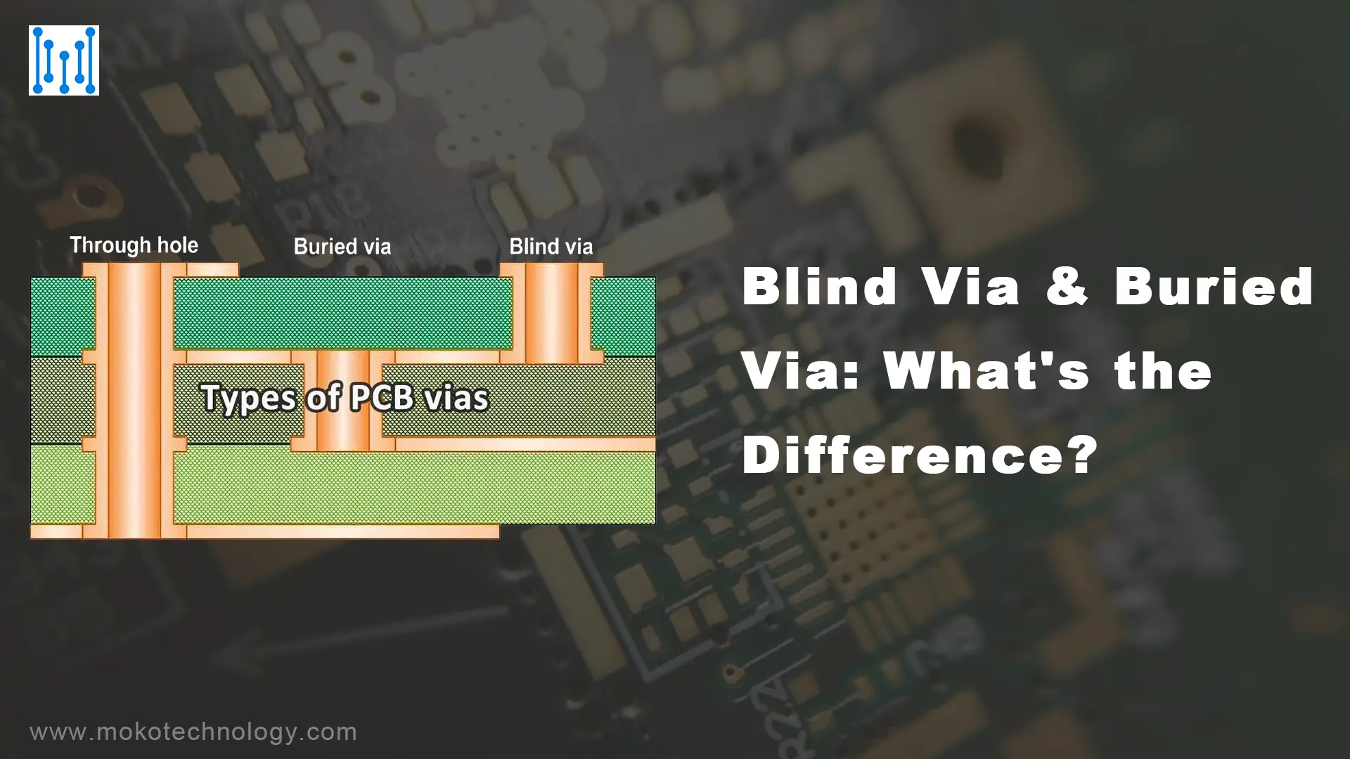
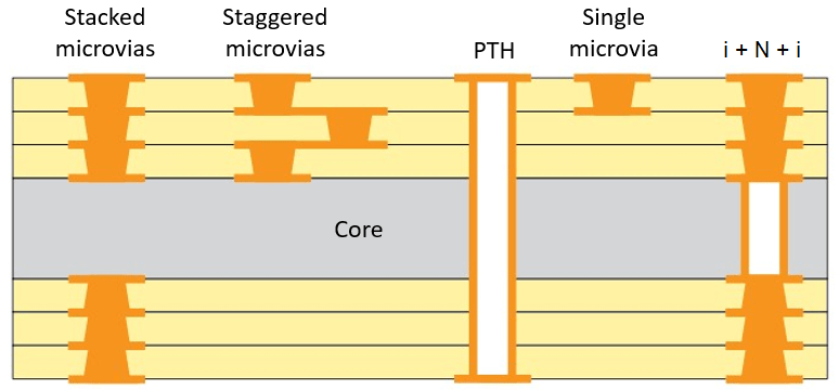
Smaller vias: HDI boards employ microvias, which can be drilled mechanically or with lasers, along with blind/buried and staggered vias for transitioning between layers. These vias have reduced aspect ratios compared to conventional through-hole vias, and their smaller diameters restrict their depth.
Thinner Traces: High-Density Interconnect (HDI) boards necessitate narrower traces for establishing connections to vias on multiple layers and in-pad vias. Thinner traces also enable higher trace density, which is a key aspect of HDI design.
Higher layer count: While non-HDI boards can have high layer counts, HDI boards often have 20 or more layers, especially when dealing with high pin density components like FPGAs. The increased layer count allows for more complex routing and interconnectivity.
Lower signal levels: HDI boards are generally unsuitable for applications involving high voltage or high current. This is because the close proximity of neighboring lines in HDI layouts can cause ESD (electrostatic discharge) issues, and high currents can result in excessive temperature rise in conductors. Thus, HDI layouts are primarily used for low voltage and low current electronic devices.
Key Considerations for HDI PCB Design
Design considerations for High-Density Interconnect PCBs often require unique production processes distinct from those used for other PCB types. The following are some of the key considerations involved in HDI PCB production:
- Layer Stackup
HDI PCBs typically have multiple layers with high-density routing and interconnects. The layer stackup is a critical consideration as it affects the overall performance and manufacturability of the PCB. Factors to consider in layer stackup include the number of layers, the thickness of each layer, the type of materials used, and the arrangement of power and ground planes. Proper layer stackup design is essential to ensure signal integrity, controlled impedance, and thermal management.
- Trace Width and Spacing
HDI PCBs require tight spacing between traces and pads to accommodate high-density routing. The trace width and spacing must be carefully chosen to meet the design requirements, such as controlled impedance, crosstalk, and current carrying capacity. Smaller trace widths and spacing may be needed to achieve higher circuit density, but they can also increase the risk of signal integrity issues, manufacturing defects, and electrical noise.
- Via Design
HDI PCBs heavily rely on vias for interconnection between different layers. Proper via design is crucial to achieving high-density routing and reliable signal transmission. There are several types of PCV vias, including through-hole vias, blind vias, and buried vias, each with its advantages and limitations. The location, size, and spacing of vias must be carefully considered to ensure proper electrical performance, thermal management, and manufacturability.
- Component Placement
The placement of components on an HDI PCB is critical to achieving high circuit density and optimized signal routing. Careful consideration must be given to the placement of components, including passive components, ICs, connectors, and other components, to minimize signal delays, routing congestion, and thermal issues. The strategic arrangement of components on a PCB can greatly influence the board’s overall performance and reliability.
- Signal Integrity
HDI PCBs often operate at high speeds, and signal integrity is crucial to ensure reliable performance. Factors such as impedance matching, signal reflections, crosstalk, and electromagnetic interference (EMI) must be carefully considered during the design phase. Advanced simulation and analysis tools can be used to validate signal integrity and optimize the PCB design for high-speed signaling.
- HDI Structures
HDI PCBs are available in various layout options, including 1-n-1 PCB and 2-n-2 PCB. A 1-n-1 printed circuit board is the most basic form of high-density interconnect PCB, composed of a single stack of interconnected layers. It involves sequential lamination on both sides of the core. On the contrary, a 2-n-2 PCB has two HDI layers, which enable staggered or stacked microvias across different layers. Complex designs often incorporate copper-filled stacked microvia structures, and the number of layers (X-n-X) can reach high levels, although complexity and cost considerations may limit the build-up.
7 Tips to Make Your HDI PCB Design a Success
- Adopt a DFM Strategy
To ensure a seamless and cost-effective manufacturing process for High-Density Interconnect (HDI) PCBs, we recommend integrating a Design for Manufacturing (DFM) strategy. This approach focuses on developing a product that can be manufactured quickly and efficiently, while also being practical and feasible.
- Consider Manufacturing Capabilities
When designing an HDI PCB, it’s crucial to take into account the capabilities of your chosen PCB manufacturer. Designing a board that goes beyond its capabilities may result in a futile design. To ensure success, create an HDI board that leverages the advantages of HDI technology while being manufacturable by your chosen manufacturer.
- Choose the Right Via Type
The type of via you choose can significantly impact production cost and time. Micro-vias, such as via-in-pad and near-pad versions, can reduce production time and cost by limiting the number of layers and materials. When selecting a via type, consider the cost for both you and your HDI PCB manufacturer, while also ensuring that it meets the required electrical performance of the HDI PCB.
- Consider Availability and Size of Components
The number and size of components used in the HDI PCB design also play a crucial role. Keep in mind that the primary objective of HDI PCBs is to minimize expenses and surface space. Choose lightweight, cost-effective, and minimal components that meet the design requirements. The placement of components will impact trace width, hole size, and overall board dimensions, so ensure quality and reliability while optimizing for space.
- Avoid Overcrowding Components
While a compact design may tempt you to place components too close to each other, it’s important to avoid overcrowding. High-powered devices can result in Electromagnetic Interference (EMI), affecting signal integrity. Additionally, inductances and capacitances near pads can impact signal strength and communication speed. Ensure components are placed to spread vias symmetrically to reduce stress and avoid distortion. Consider ease of maintenance and rework during installation stages.
- Choose an Efficient Stackup Design
The stackup design of the PCB can also impact manufacturing challenges. The number of layers and material types in the stackup can affect the laminate frequency and drilling time. Choose a stackup design that is efficient yet cost-effective, taking into consideration the manufacturing capabilities of your chosen PCB manufacturer.
- Work with A PCB Design Expert
If you’re designing an HDI PCB, it’s important to work with a PCB design expert. A design expert can help you plan out your layout, select the right materials, and ensure your design is optimized for performance and manufacturability. When choosing a PCB design expert, look for someone who has experience with HDI layout and has a proven track record of success.
Conclusion
In conclusion, HDI PCB design is a critical process that requires careful consideration of various factors. By following the HDI PCB design guidelines and considering the key factors mentioned in this blog, designers can create innovative and reliable HDI designs and enable the realization of innovative and cutting-edge products. MOKO Technology, a leading PCB manufacturer in China, has been engaged in PCB design for nearly 20 years. We own all expertise and tools required to complete powerful HDI PCB design, our team of experts has served customers from various industries ranging from medical, and consumer electronics, to automotive, and IoT. Contact us to get reliable HDI PCB design services.