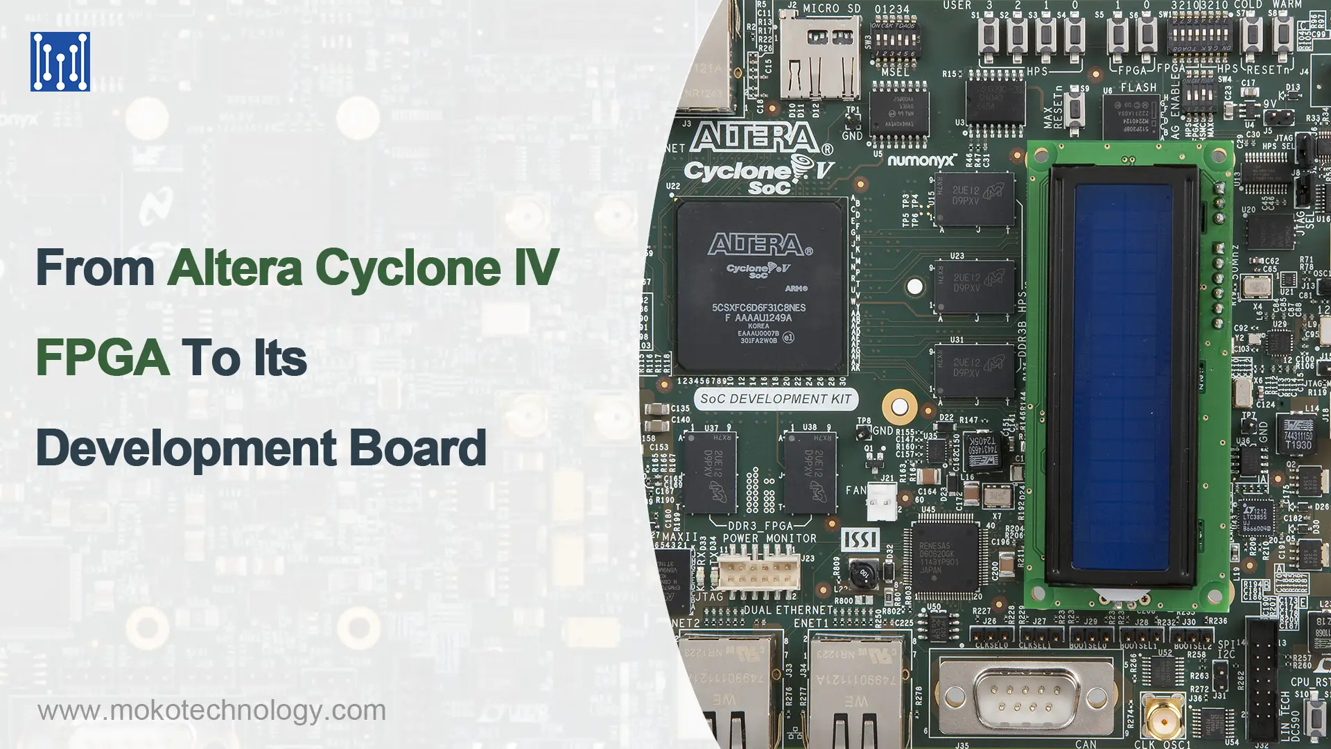
The modern electronic manufacturing field witnesses the popularity of Altera Cyclone IV FPGA development board. This text will brief you on something important from Altera Cyclone IV FPGA to its development board, including chip specification, chip features, the approach to getting board with that chip, the question on making board with Altera Cyclone IV FPGA and some highly recommended Altera Cyclone IV FPGA PCB. Ok , now let’s dive into these.
Specification of Altera Cyclone IV FPGA
| Item | Logic Elements | Digital Signal Process Module | Maximum Embedded Memory | Maximum User I/O | Package Option |
| EP4CE6 | 6000 | 15 | 270Kb | 179 | E144, U256,F256 |
| EP4CE10 | 10000 | 23 | 414 Kb | 179 | E144, U256, F256 |
| EP4CE15 | 15000 | 56 | 504Kb | 343 | E144,M164,U256,M256,F256,F484 |
| EP4CE22 | 22000 | 66 | 594 Kb | 153 | E144, U256, F256 |
| EP4CE30 | 29000 | 66 | 594 Kb | 532 | U484, F324, F484, F780 |
| EP4CE40 | 40000 | 116 | 1.134 Mb | 532 | U484, F324, F484, F780 |
| EP4CE55 | 56000 | 154 | 2.34 Mb | 374 | U484, F484, F780 |
| EP4CE75 | 75000 | 200 | 2.745 Mb | 426 | U484, F484, F780 |
| EP4CE115 | 114000 | 266 | 3.888 Mb | 528 | F484, F780 |
| EP4CGX15 | 14000 | 0 | 540 Kb | 72 | F169 |
| EP4CGX22 | 21000 | 40 | 756 Kb | 150 | F169, F324 |
| EP4CGX30 | 29000 | 80 | 1.08 Mb | 290 | F169, F324, F484 |
| EP4CGX50 | 50000 | 140 | 2.502 Mb | 310 | F484, F672 |
| EP4CGX75 | 74000 | 198 | 4.158 Mb | 310 | F484, F672 |
| EP4CGX110 | 109000 | 280 | 5.49 Mb | 475 | F484, F672, F896 |
| EP4CGX150 | 150000 | 360 | 6.48 Mb | 475 | F484, F672, F896 |
Features of Altera Cyclone IV FPGA
Two Sub-series Available
Altera Cyclone IV FPGA comes with two sub-series. One is E series, the other is GX FPGA. While E range features typical static power consumption, GX range offers lower price and integration design to users. It aims at meeting different demand in the market as much as possible.
Less Cost of PCB
All type of thip in Cyclone IV FPGA family only requires two batteries, leading to distribution network simplification, low-cost PCB, space-saving PCB and short design time. The integrated transceiver on FPGA framework greatly contributes to the integration of main board design. Besides, flexible framework of transceiver clock is compatible to various protocol, when it makes full use of all available resources.
In addition, the chip of Cyclone IV GX range does well in space saving so as to apply to small printed circuit board with lower cost.
Optimized Framework
Thanks to pioneering processing technique applied on handheld device, Cyclone IV reduce current leakage and decrease static power. Moreover, it exploits many strengthen technique and framework, including low dielectric constant material, variable channel length and oxide thickness, and multi-transistor threshold voltage.
Integrated Transceiver
Cyclone IV GX FPGA is equipped with perfect transceiver technique, which is famous for jitter performance and excellent signal integrity. What’s more, it distinguish itself by compatibility to various serial protocol. Last but not least, it is applicable to PCI Express x1, x2 and x4 in root port and endpoint configuration with its Intellectual Property (IP) core modules.
How Can I get Altera Cyclone IV FPGA Development Boards?
Order Chips From Intel or Xilinx
You will get a kit with all the components to make a FPGA board from Intel or Xilinx. However, capacitors for decoupling, resistor for test points and low-power resistors should be prepared by yourself. With the readiness of PCB components and design, you can work out a perfect Altera Cyclone IV FPGA development boards.
Order A Bare Board With Cyclone IV Chips and Assembly on Your Own
You will get a board with logic and transceiver blocks, but no designs. It is very convenient for designers to add optional components and build a complete platform for testing board features.
Order FPGA Boards With Cyclone IV Chips From Board Assembly House
You will get a complete FPGA board design, embedded design, required components and assembled Cyclone IV FPGA board from board assembly house.
Common Problems When Working for Altera Cyclone IV FPGA Development Boards
Normal Current Should Go Through PLL VCCA
The bottom pad of EP4CE6E22 packed via T144 has been connected to the ground. After connecting to battery, the board performs normal. However, after connecting to FPGA and configuration, the auto detection results via QUARTUS shows disability to scan the device chain. Meanwhile, JTAG Debugger suggests incorrect clock valve. It seems that the chips are disconnected. Last but not least, multi-meter shows that there is no short cut among four ground resistors for JTAG.
A: Low pass filter has been added before PLL VCCA with excessive resistor. This result in only 0.6 voltage between ends of PLL VCCA. However, according to handbook, we should allow normal current through VCCA of PLL no matter we use that VCCA or not. Thus, the right solution is reducing the resistor of filter to 0 Ohm.
Bonding Pad of Download Circuit Should Be Connected To the Ground
One one hand, JTAG is downloaded and the program runs in normal, but there is something wrong with the download of JIC file of JTGA. On the other hand, ASP is rightly downloaded, but the program can not loading when power is on.
Pull-up resistors and pull-up resistors and their soldering is OK. Quartus 13.1 and programming running is good. There is no problem on the chip and chip soldering. The power supply to the chip also works well. Oscillator is in good status, too.
A: There must be some problem on the download circuit. Probably, the reason why JTAG can work well but the device can not program is that three signals on download circuit is wrong. The handbook of EP4C tell that one of the signal should be connect to the ground by resistor. So, refer to the related chapter on the handbook and change your assembling.
The interface of JTAG Should Be Function Well When Taking JTAG Debugging
When debugging the Altera Cyclone IV FPGA development boards, it shows the following errors.
!Error: JTAG chain problem detected
!Error: TDI connection to the first detected device EP3C(10|5)/EP4CE(10|6) might be shorted to GND
!Error: The TCK and TMS connections to the device before the first detected device EP3C(10|5)/EP4CE(10|6) might have a problem
!Info: Detected 1 device(s)
!Info: Device 1: EP3C(10|5)/EP4CE(10|6)
A: We advise to detect the problem of JTAG IC programming interface. The soldering may be disconnected or short cut.
Top 3 Altera Cyclone IV FPGA Development Boards
1. Development Boards for IV Video Image
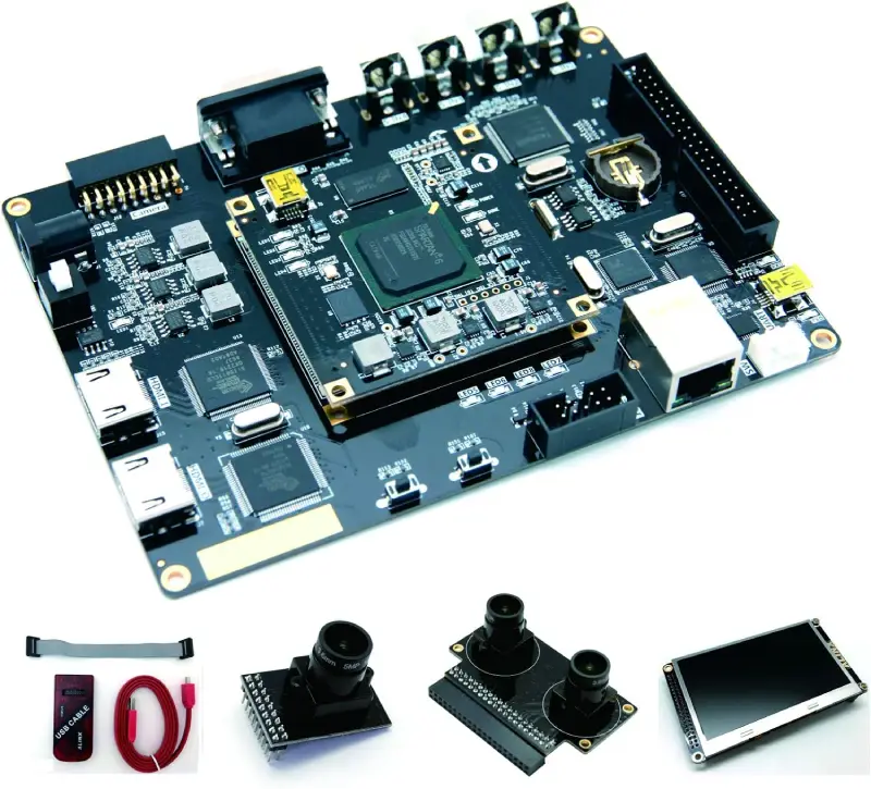
- FPGA: ALTERA Cyclone IV EP4CE75F23C8, 64*32bit DDR2 memory,126M 9K RAM
- HDMI Input/ HDMI Output/ VGA Output/ Gigabit Ethernet/ CMOS Camera Interface/ ARM SWD Debug Interface/ FPGA JTAG Debug Interface
- Provide schematic in PDF, instruction manual and VHDL examples
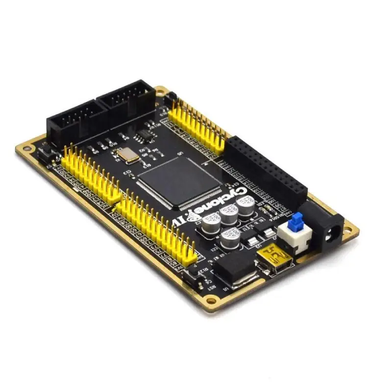
2. Development Boards for Bluetooth Video Card
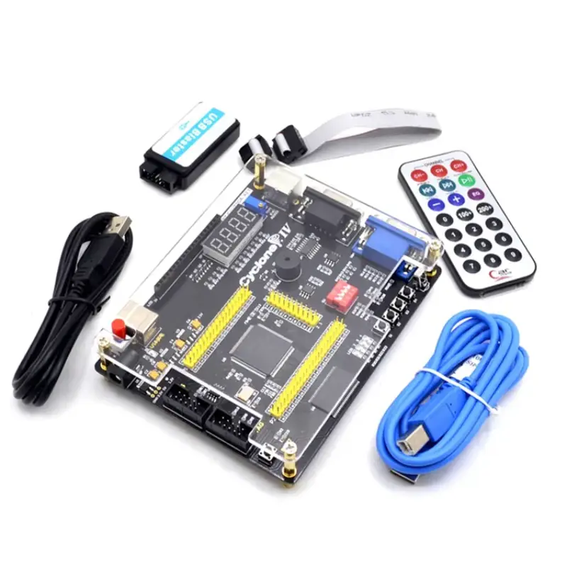
3. Development Boards for USB Blaster Download and Infrared Control
Takeaway
Altera Cyclone IV FPGA is exactly a useful chip family in electronic manufacturer field. If you want development board with this chip, feel free to contact us.