Impedancia a juego: A Critical Factor in High-Speed PCB Design

Impedance matching has become a cornerstone of the integridad de la señal in the realm of PCB de alta velocidad diseño. Future electronic devices are approaching the speed and performance boundaries, and distortion and reflection must be kept to an absolute minimum. En este blog, we will discuss in detail what impedance matching is all about, its necessity and how to achieve it in PCB design.
What Is Impedance Matching?
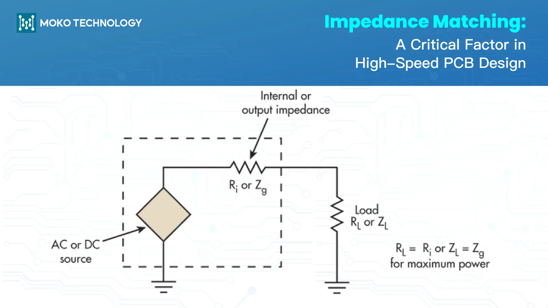
Impedance matching is the practice that makes sure the load impedance matches the characteristic impedance of the transmission line in a in circuit board. Such an alignment eliminates signal reflections, so energy will be fully absorbed by the load without distortion or loss. In PCB design, impedance is the total opposition that a circuit offers to an alternating current, and it’s measured in ohms or Ω (ohm). If the impedances are mismatched, some part of the signal will be reflected back, which would cause several issues like signal distortion, overshoot and ringing.
Difference between Controlled Impedance and Impedance Matching
When we are talking about the impedance matching, the term that comes to our mind is impedancia controlada. Are they two separate objects or are they aliases of each other? De hecho, they are for other purposes.
Controlled impedance always aims to have the same impedance in the transmission line for it by using proper trace geometry and material selection. Impedance Matching seeks to transfer maximum power across the linked components through alignment of source and load impedances.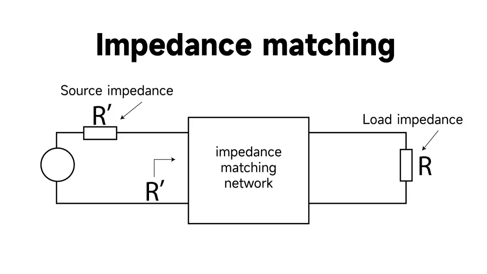

Why Is Impedance Matching Critical in High-Speed PCB Design?
Impedance matching is very important in high speed PCB design for resolving most fundamental signal integrity challenges. The signal is clean when impedances are properly matched between components and transmission lines, because the signal reflections causing the degradation and distortion are minimized. Adicionalmente, the matched impedances give utmost power transfer between connected elements, to minimize loss of energy, which is very important in high frequency applications. Además, impedance matching also ensures the signal integrity free from ringing and overshoot. In high frequency and RF systems, transmission line effects are significant and even small mismatch has considerable effect on performance such that the system can fail or be unreliable.
Key Factors Affecting Impedance Matching
The following factors produce an effect on impedance matching during PCB design:
- Trace Geometry: The dimensions of PCB traces should receive detailed attention when designing since they directly influence impedance levels. Wider traces decrease impedance and thinner ones increase it.
- Materiales: The most important requirement for successful impedance control lies in the selection of PCB substrate material. For standard designs, FR-4 is a suitable material but Rogers laminates are preferred for frequency demanding designs.
- Reference Planes: The distance between the trace and the reference plane affects impedance as well. Impedance decreases when planes approach each other yet it rises with greater separation distances.
- Propiedades dielectricas: The value of constante dieléctrica(εr) in PCB materials affects the signal propagating behavior and impedance. Higher dielectric constant decreases impedance but they might result in signal attenuation.
- Signal Rise/Fall Time: The speed of signal edges affects impedance control because fast signal edges (short rise or fall times) need tighter impedance management to stop reflection effects and signal deterioration.
5 Methods to Achieve Impedance Matching in PCB Design

The implementation of particular techniques becomes essential for achieving successful impedance matching during PCB design. Aquí están 5 effective approaches:
- Optimize Trace Width and Spacing: The width and spacing dimensions of PCB traces determine how impedance develops in the system. Specialized software enables designers to perform calculations for these parameters while they must account for dielectric constant and copper thickness to achieve proper impedance values.
- Select Suitable Dielectric Materials: The laminate material of PCB should be selected with controlled dielectric properties, which can provide uniform impedance features across the entire PCB. The selected materials reduce fluctuations in performance which occur because of temperature and humidity changes.
- Develop Strategic Layer Architecture: A strategic layer stack-up is essential for impedance management because it directly contributes to impedance control. Signal layers should be placed between ground planes, so as to create stable return paths which decrease crosstalk and establish uniform impedance.
- Apply Termination Techniques: Applying terminal techniques is a useful methods to enhance signal impedance matching, which can also reduce the signal reflections. As to which method to use, series or parallel termination? You should choose it based on circuit requirements together with transmission line characteristics
- Integrate Impedance Matching Networks: Engineers integrate impedance matching networks by adding resistors, capacitors and inductors while designing the PCB. These networks function strategically to match impedance values between the source and transmission line and load.
Conclusión
For successful high speed PCB design, impedance matching still plays a crucial role in ensuring signal integrity, efficient power transfer, and it also helps to reduce the electromagnetic interference. This blog provide insights on how to achieve impedance matching in PCB and highlights the design considerations that engineers should consider throughout the development process. MOKO Technology provides PCB design and manufacturing services while dedicating exceptional focus to impedance matching standards. If you are still confused about PCB impedance matching, comuníquese con nosotros—our experts are here to help.


Mensajes recientes
How to Clean a Circuit Board Safely and Effectively?
It is important to learn how to clean a circuit board properly if you’re working…
Counterbore vs Countersink: Which to Choose for Your PCB?
When designing PCBs, selecting the appropriate type of holes for fasteners is crucial. And much…
PCB Copper Foil: Tipos, Propiedades & Como escoger
PCB copper foil is one of the most critical materials in the printed circuit board…
MOKO Technology Launches Vietnam Manufacturing Base in February 2025
Shenzhen, China - febrero 11, 2025 - Tecnología MOKO, a leading global electronics manufacturing service…
PCB Solder Mask: What It Is and Why Every Circuit Board Needs It?
While most people focus on the components and copper traces that make up PCBs, there's…
Aluminum PCB vs FR4 PCB: Key Differences and How to Choose?
The right type of PCB material can make or break the performance of your electronics project.…