How to Design PCB Antenna Like a Pro?

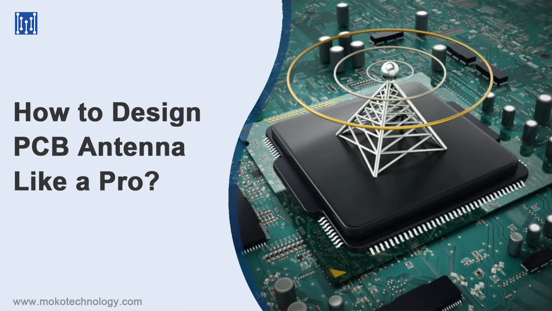
Antennas play a critical role in any wireless system, which is used to transmit and receive electromagnetic signals that carry data. As electronics continue getting smaller, engineers have developed ingenious antenna designs that integrate directly onto printed circuit boards. Known as PCB antennas, these compact antennas provide numerous benefits over traditional protruding antennas. In this blog, we’ll dive into PCB antenna fundamentals, walk through the design process, and explore layout guidelines so you can design PCB antennas like a pro!
What Is a PCB Antenna?
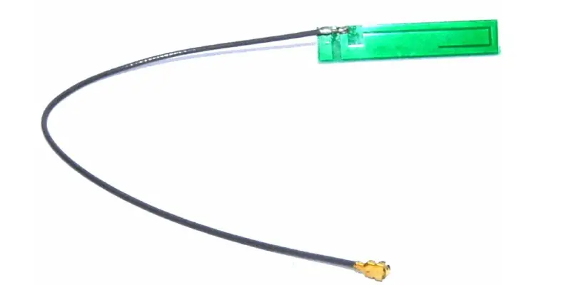
A PCB antenna, or printed circuit board antenna, is an antenna integrated directly onto a PCB board. By printing antennas directly onto circuit boards, PCB antennas eliminate the need for external antenna structures, save space, reduce assembly costs, and enable sleek, low-profile products. So how do PCB antennas work exactly? PCB antennas function using the same fundamental antenna principles as other types. The conductive traces on the PCB act as radiating elements that convert currents into electromagnetic waves. The shape and layout of these traces determine the antenna radiation pattern.
Types of Antenna on PCB
- Monopole Antenna
Monopole antennas are simple and easy to implement, they are often used for low-frequency applications like Bluetooth and Wi-Fi.

- Patch Antenna
Ideal for higher frequencies, patch antennas are commonly used in GPS modules and wireless communication systems.
- Inverted-F Antenna(IFA)
A compact and versatile option, IFA is often employed in smartphones and wearables due to its excellent performance.
- Dipole Antenna
Offering bidirectional radiation patterns, dipole antennas are suitable for certain wireless communication systems.
- Loop Antenna
The loop antenna is a simple and widely used PCB design, which is valuable as a receiver, especially for radio direction finding (RDF) to locate transmitters due to its directional pattern.
- Slot Antenna
Slot antennas get their name from their unique design, which involves a metal plate with multiple slots or cuts. They are commonly used in applications like aircraft radars and phased arrays.
Essential Steps for Successful PCB Antenna Design and Layout
-
Define Your Requirements and Goals
Identify the frequency range, data rate, coverage area, and any other relevant specifications. Additionally, consider environmental factors such as temperature, humidity, and interference sources that could affect antenna performance.
-
Choose the Right Antenna Type for Your Application
There are various factors that need to be considered when choosing the antenna type such as the frequency of operation, radiation pattern requirements, and physical constraints. Each antenna type has its advantages and limitations, consider your specific application needs and select the antenna type that aligns best with your requirements.
-
Utilize Tools and Software for PCB Antenna Design
Modern design tools and simulation software play a critical role in optimizing antenna performance. Utilize tools like Computer-Aided Design (CAD) software and electromagnetic simulation software to model and simulate your antenna designs. These tools allow you to visualize the radiation patterns, analyze impedance matching, and evaluate the overall performance of your antenna. By leveraging simulation, you can make informed design decisions and avoid costly mistakes in the physical prototyping stage.
-
Optimize PCB Material Selection for Antenna Performance
The choice of PCB material can significantly impact the performance of your antenna. The dielectric constant and loss tangent of the PCB material influence the impedance matching and radiation efficiency. Higher dielectric constants can increase the antenna’s physical size, while higher loss tangents can lead to reduced signal propagation. Choose a PCB material with a dielectric constant suitable for your frequency of operation, and keep the loss tangent as low as possible to minimize signal losses.
-
Ensure Effective Ground Plane Design for Improved Radiation Patterns
A well-designed ground plane is crucial for the proper functioning of a PCB antenna. The ground plane acts as a reference point for the antenna’s radiation, and its size and shape influence the radiation patterns. For monopole and inverted-F antennas, the ground plane serves as the second element of the antenna. Ensure that the ground plane is large enough to provide a low-impedance path for the return currents. A ground plane with low resistance and low inductance helps in achieving a better radiation pattern and reduces EMI.
-
Carefully Position the Antenna and Nearby Components
The physical placement of the antenna on the PCB will affect its performance. Avoid placing the antenna near metal objects, other high-frequency components, or sources of interference. Components such as metal shielding, connectors, and large capacitors can alter the radiation patterns and impedance of the antenna.
-
Consider Signal Traces and RF
The routing of signal traces on the PCB, especially high-frequency traces, can impact antenna performance. Avoid running signal traces too close to the antenna, as it can lead to coupling and detuning the antenna. Use proper RF design techniques, such as controlled impedance traces and microstrip/stripline routing, to ensure signal integrity and minimize losses.
-
Implement Impedance Matching Techniques for Efficiency
Impedance matching is essential for maximizing power transfer from the RF circuitry to the antenna. Proper impedance matching ensures that the RF energy is efficiently radiated by the antenna. Techniques like L-section matching networks, quarter-wave transformers, or series capacitors can be used to achieve impedance matching. Simulations and testing are vital in fine-tuning the matching network to achieve optimal performance.
-
Tune and Test the PCB Antenna for Optimal Performance
Conduct practical tests on the physical prototype to validate the performance. Use a network analyzer or spectrum analyzer to measure the antenna’s return loss, radiation pattern, and gain. Make iterative adjustments to the design based on the testing results to achieve the desired specifications.
-
Mitigate Electromagnetic Interference (EMI) Issues
EMI can adversely affect antenna performance and overall circuit operation. To reduce EMI, incorporate proper shielding and filtering techniques. Shield sensitive circuitry from external interference sources and minimize the generation of unintended electromagnetic emissions from the antenna. Proper filtering can also help reduce noise and improve signal quality.
Tips for Better PCB Antenna Design
Aside from the initial antenna design, there are several methods to enhance the efficiency and optimize the output of PCB antennas. Some of these techniques include:
- Implementing Matching Networks: Incorporating matching networks during tuning helps compensate for factors that may impact the antenna’s overall performance.
- Choosing an Appropriate Ground Plane: Selecting the right ground plane is crucial to avoid crosstalk between signals. And it’s recognized that putting the antenna at the edge of the PCB is agood choice
- Avoiding Metal Casing: To prevent signal disruption, it is important not to encase the antenna in metal. Signals cannot travel through metal, and enclosing the antenna in such material can lead to interference.
- Positioning Away from Plastic Surfaces: Placing the antenna near plastic surfaces can negatively affect its performance. Plastic has a higher dielectric constant than air, resulting in signal dampening and losses. This increases the electrical length of the antenna and reduces its radiating frequency.
- Opting for High-Quality FR4 Circuit Boards: To maintain optimal RF performance, it is recommended to use high-qualityFR4 circuit boards. These boards can help avoid issues that may arise with RF signals.
PCB antennas have clearly become a critical technology for enabling wireless functionality in small products. By following the guidelines outlined in this blog, you’ll be designing tiny, capable PCB antennas like a pro in no time. Or you can contact our experts, they would be happy to discuss more details and provide guidance for your specific project needs.


Recent Posts
Impedance Matching: A Critical Factor in High-Speed PCB Design
Impedance matching has become a cornerstone of the signal integrity in the realm of high speed PCB…
How to Clean a Circuit Board Safely and Effectively?
It is important to learn how to clean a circuit board properly if you’re working…
Counterbore vs Countersink: Which to Choose for Your PCB?
When designing PCBs, selecting the appropriate type of holes for fasteners is crucial. And much…
PCB Copper Foil: Types, Properties & How to Choose
PCB copper foil is one of the most critical materials in the printed circuit board…
MOKO Technology Launches Vietnam Manufacturing Base in February 2025
Shenzhen, China - February 11, 2025 - MOKO Technology, a leading global electronics manufacturing service…
PCB Solder Mask: What It Is and Why Every Circuit Board Needs It?
While most people focus on the components and copper traces that make up PCBs, there's…