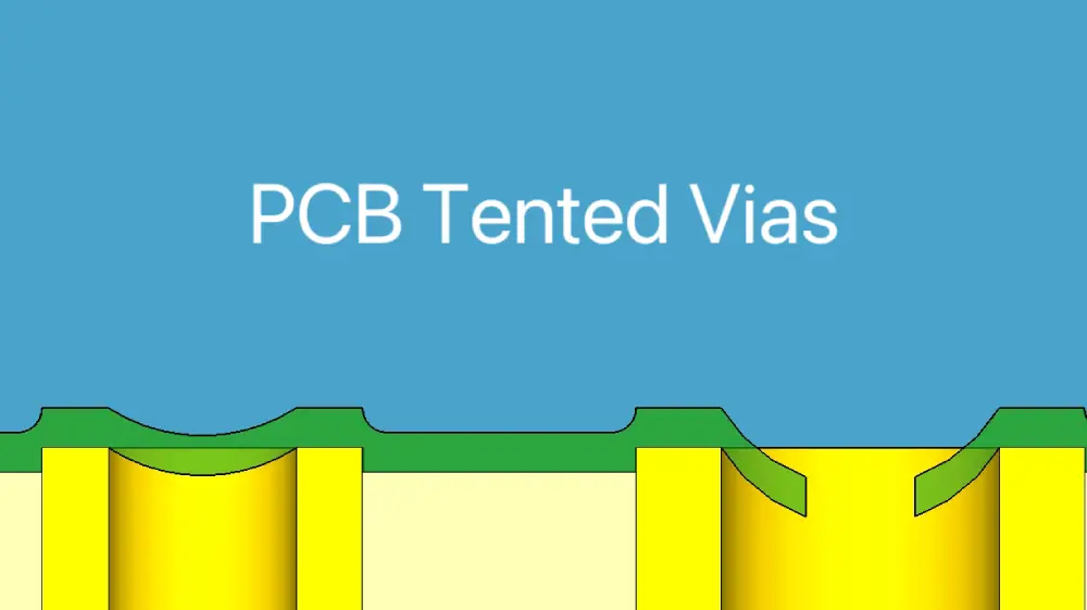
Unter PCB-Durchkontaktierungen versteht man kleine Löcher, die in die Leiterplatte gebohrt werden, um eine Verbindung zwischen verschiedenen Schichten auf der Leiterplatte herzustellen. Während PCB Wege sind entscheidend für die Gesamtfunktionalität von Leiterplatten, mit ihnen sind Probleme verbunden, einschließlich ihrer Anfälligkeit gegenüber Schadstoffen sowie der Möglichkeit einer Entwicklung Lötbrücken während der Montagephase. Hier kommt PCB via Tenting zum Einsatz. Beim Via-Tenting wird eine Lötmaske verwendet, die die Via-Löcher abschirmt, um zu verhindern, dass während der Lötphase Lot in sie hineinfließt. In diesem Artikel, Wir werden etwas über seine Vorteile erfahren, über Techniken gezeltet, und Designüberlegungen.
Was ist PCB Via Tenting??
PCB Via Tenting ist eines der Verfahren, bei denen Teile von Durchkontaktierungen abgedeckt werden oder man sagen kann, dass sie abgeschirmt sind. Vias sind plattierte Löcher in der Leiterplatte mit kleinen Öffnungen, die elektrische Verbindungen zwischen Schichten der Leiterplatte herstellen und normalerweise auf der Oberfläche der Leiterplatte freiliegen. Der Grund für die Verwendung von Via-Tenting besteht darin, sicherzustellen, dass diese Vias physisch abgeschirmt sind, um ungeschützte Bedingungen zu vermeiden, die zu bestimmten Umwelt- oder Stromkatastrophen führen können. Auftragen eines Materials, das sich wie eine Lötmaske anpasst, Epoxid oder Polyimid deckt die freiliegenden Metalloberflächen der Vias ab und isoliert diese so.
Vorteile von PCB Via Tenting
-
Schutz vor Kontamination
PCB-Durchkontaktierungszelte tragen dazu bei, die Durchkontaktierungslöcher vor Situationen wie Staub zu schützen, Feuchtigkeit, und andere Schadstoffe aus der Umwelt. Dieser Schutz ist in der Tat unerlässlich, um das Korrosionsrisiko zu verringern und eine lange Lebensdauer der Leiterplatte zu gewährleisten.
-
Verhinderung von Lötbrücken
Das Abdecken der Durchkontaktierungen mit einer Lötstoppmaske könnte die Durchkontaktierungen auch im anschließenden Montageprozess vor dem Lotfluss schützen. Dies minimiert die Wahrscheinlichkeit, dass sich Lötbrücken über den Verbindungsstellen bilden, um die elektrische Verbindung zu verbessern, und minimiert auch die Wahrscheinlichkeit, dass Lötzinn eine Brücke über andere Bereiche bildet, was zu Verkürzungen oder anderen Formen von Defekten führt.
-
Verbesserte elektrische Leistung
Zelte tragen dazu bei, die Durchkontaktierungen vor Beschädigungen durch Verunreinigungen und Lot zu schützen, da sie die gewünschten Leiterbahnen abdecken. Dies führt zu einem gleichmäßigeren elektrischen Verhalten, was zu einer besseren Leistung bei gleich höheren Frequenzen führte.
-
Verbessertes Wärmemanagement
Obwohl Zelte einen geringen Einfluss auf die Wärmeableitung haben können, zur selben Zeit, Es hilft bei der Ermittlung der erforderlichen thermischen Eigenschaften der Leiterplatte und bietet somit eine zusätzliche Schutzschicht. Dies ist insbesondere in Anwendungsbereichen wie Hochspannung und Strom erforderlich, in denen die Wärmeableitung von größter Bedeutung ist.
-
Verbesserte mechanische Festigkeit
Der Lötstopplack hat auch mechanische Vorteile: Es schirmt die Vias ab und macht sie widerstandsfähiger gegen mechanische Belastungen, denen eine Leiterplatte bei der Montage ausgesetzt sein kann.
Verschiedene Tented-Via-Techniken
| Komplettes Zelten
|
Bei dieser Technik werden die oberen und unteren Schichten der Leiterplatte mit einer Lötmaske beschichtet, Dadurch kann die Durchkontaktierung effektiv vor anderen Elementen geschützt und für die beste Isolierung gesorgt werden.
|
| Teilweises Zelten
|
Wenn teilweises Zelten eingesetzt wird, Nur eine der Schichten der Leiterplatte wird mit der Lötmaske beschichtet, während die andere Seite frei bleibt; Dies ist besonders nützlich, wenn eine Wärmeableitung durch die Durchkontaktierung erforderlich ist oder ein Zugang erforderlich ist.
|
| Zelten mit Coverlay
|
Bei dieser Technik wird Coverlay verwendet, ein flexibles dielektrisches Material anstelle einer Lötmaske; Starrflex bzw flexible Leiterplatten werden in der Regel aus diesem Material hergestellt.
|
| Zelten mit Kappenstopfen
|
Bei dieser Methode wird die Durchkontaktierung zunächst mit einer Schicht Lötstopplack abgedeckt und anschließend mit einem nichtleitenden Material wie Harz oder Epoxidharz gefüllt, um die gesamte Durchkontaktierung einzukapseln. Als Ergebnis, Es verbessert den Schutz vor Umwelteinflüssen und mechanischen Belastungen.
|
| Zelt mit Kupferfüllung
|
Beim Bilden einer Durchkontaktierung unter einer Schicht Lötstopplack, anstatt dass die Durchkontaktierung praktisch leer ist, Es kann eine Kupferfüllung verwendet werden, die sowohl die strukturelle Unterstützung als auch die thermischen Fähigkeiten der Durchkontaktierung ergänzt.
|
| Über Stecker
|
Neben dem Aufbringen einer Lötmaske auf die Durchkontaktierung ist es auch möglich, die Durchkontaktierung mit leitendem oder nicht leitendem Material zu füllen, um sie zu verschließen; Diese Form wird häufiger verwendet in Leiterplatten mit hoher Verbindungsdichte wo der Platz entscheidend ist.
|
Designüberlegungen für Tented Via
-
Art und Material der Lötmaske
Art und Material der Lötmaske sind weitere entscheidende Faktoren, die bei der Gestaltung von Tented Vias berücksichtigt werden müssen. Das Lötmaskenmaterial der Leiterplatte sollte kompatibel sein, und die Wahl der Verwendung von a Flüssigkeit fotoabbildbar (LPI) Lötmaske Alternativ kann eine Trockenfilm-Lötmaske für die Leiterplatte gewählt werden.
-
Über Größe und Seitenverhältnis
Der Durchmesser des Vias und sein Seitenverhältnis (Verhältnis von Tiefe zu Durchmesser) ist ein weiterer wichtiger Faktor, den es zu berücksichtigen gilt. Allgemein, Je kleiner der Durchmesser des Vias ist, desto einfacher ist das Zelten; und das Seitenverhältnis muss innerhalb der Fertigungsmöglichkeiten liegen.
-
Padgröße und Abstand
Designer sollten einen ausreichenden Pad-Durchmesser um die Durchkontaktierung herum belassen und sicherstellen, dass zwischen der hergestellten Durchkontaktierung und anderen Pads oder Leitungen ausreichend Platz vorhanden ist, um eine Fehlausrichtung der Maske zu vermeiden.
-
Platzierung und Dichte
Diese Durchkontaktierungen sollten nicht zu nah an den Komponenten oder anderen Durchkontaktierungen gehalten werden, da die Maskenhaftung ein Problem darstellt, und auch, Auch die Dichten der Durchkontaktierungen sollten nicht zu hoch sein, um mögliche Schwierigkeiten einer gleichmäßigen Auftragung des Lötstopplacks in den Griff zu bekommen.
-
Elektrische Leistung
Der Einfluss von Tented Vias auf die Signalintegrität, insbesondere in Hochfrequenzschaltungen, sollte beurteilt werden, Überlegen Sie, ob sich Zeltbildung auf die elektrischen Eigenschaften der Durchkontaktierung, wie z. B. die Kapazität, auswirkt.
-
Thermisches Management
Der Einfluss von Tenting-Durchgangslöchern oder Durchkontaktierungen auf die Steuerung des Wärmemanagements der Leiterplatte sollte ermittelt werden, um eine falsche Ausrichtung von thermischen Durchkontaktierungen oder Durchkontaktierungen zu vermeiden Temperatur fällt