Beim Entwurf der Leiterplatte, Ein hohes Maß an Aufmerksamkeit wird auf die PCB-Signalintegrität gelegt, also auf die Qualität der Signale in einem System und deren Wirksamkeit. Poor signal integrity can cause data error, Elektromagnetische Interferenz, and even system failure. jedoch, as devices become faster and more compact in size, the issue of signal integrity faces the utmost difficulty in optimization. In diesem Artikel, we will explore the key factors that impact PCB signal integrity and provide tips on how to enhance it during the design process. Gut, to begin with, we need to know what signal integrity in PCB design simply means in the real sense.
What Is Signal Integrity in PCB?
Signal integrity in printed circuit boards is the quality of electrical signals being transmitted and received through that PCB board. It includes the signal’s ability to maintain various electrical features, such as voltage, Zeit, and waveform from the source to the destination. Signal integrity is very important as it guarantees the correct transmission of data and the correct functioning of circuits. This is important in high-speed design and large signal paths, networks, or systems wherein every small depreciation in signal quality will appreciably affect the system’s performance.
Key Factors That Affect PCB Signal Integrity
- Trace Impedance
Impedance should be consistent throughout the length of a trace as the signal can reflect and get attenuated when impedance changes. Other parameters such as trace width and spacing have to be controlled the same to avoid distortion of the signal.
- Crosstalk
Crosstalk is a form of electromagnetic interference where signals in adjacent or nearby traces couple into each other, potentially corrupting data. The severity of crosstalk depends on factors such as the length of the traces running in parallel, their proximity to each other, and the overall PCB layout.
- Signal Reflection
Reflection occurs when the impedance of the trace and that of the load or source differ thus distorting the signal. Such discrepancies are commonly observed due to differing Spurbreite, Dielektrizitätskonstante, or sudden changes in the signal’s route.
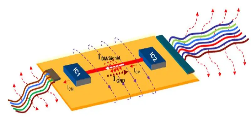
- Elektromagnetische Interferenz (EMI)
Intrusive noise is also brought about by EMI from external sources into the PCB signals. External electromagnetic fields can get coupled into the PCB traces particularly in the areas of large loop areas or poor shielding.
- Leistungsintegrität
A stable power supply is essential when it comes to signal quality since the signals and fields generated may be disrupted if power varies. Electrical signal power supply anomalies may cause noise or distort the desired signals on high speed data lines.
- Leiterplattenmaterial
The dielectric constant and loss tangent des PCB-Materialien have an influence on the signal speeds and the levels of attenuation. jedoch, fluctuation in material properties poses a problem, especially in high-frequency applications.
- Trace Length and Routing
When the traces for the differential pairs and other high-speed signals have equal length, then they arrive at the receiver at the same time and therefore minimize skew. Differing trace lengths and sharp angles are likely to bring reflection difficulties and signal degradation.
Design Tips to Improve PCB Signal Integrity
While it is impossible to ensure that the signal is completely free of distortion, some PCB design tips can help minimize any potential signal distortion and enhance the signal integrity in PCB:
-
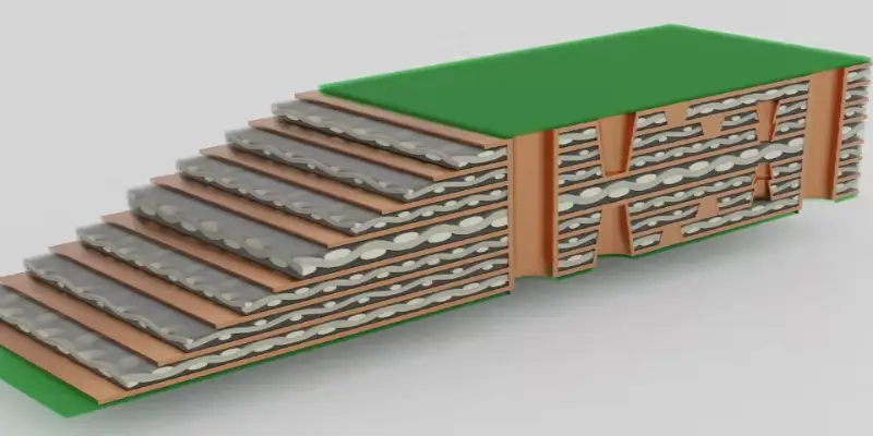
Proper Layer Stackup
Signal layers must be placed in close proximity to ground planes as this aids in the management of the impedance as well as preventing crosstalk. Allgemein, the high-speed signals should be laid on inner layers between the ground planes to provide isolation from the interfering signals.
Weiterführende Literatur: Richtlinien für das PCB-Stackup-Design
-
Trace Routing Techniques
Trace length should not be very long as this will cause signal reflections. And we should also avoid using sharp bends. It is better to use relatively smooth curves or better yet 45-degree turns, instead of sharp 90-degree turns as smooth curves are less destructive of the signal. Ebenfalls, differential pairs should be routed together with a consistent spacing to maintain impedance and reduce noise.
-
Grounding and Decoupling
A solid ground plane is essential for reducing electromagnetic interference (EMI) and providing a stable reference for signals. The skillful decoupling with the capacitors placed close to power pins allows for ‘blocking’ the noises in the power supply line and improving the signal-delivering quality. Ground connection must be low impedance and provide adequate return paths for high-speed signals.
-
Kontrollierte Impedanz
Ensuring kontrollierte Impedanz for critical signal traces helps maintain signal quality. This involves calculating and maintaining consistent trace width, Abstand, and dielectric thickness according to the required impedance. It is recommended to employ simulation tools used for the verification of impedance with the purpose of finding potential problems on impedance before fabrication.
-
Minimize Crosstalk
To minimize the crosstalk, it is required to place sufficient distance between signal traces particularly where high-speed signals are involved. Use ground or power planes to separate signal layers, and consider using guard traces (grounded traces) between high-speed lines to further isolate them.
-
Use of Vias
It is suggested to minimize the use of vias in high-speed signal paths since they contribute to inductance and cause reflections. If vias are required, then use Rückbohren to eliminate disabled segments of the via barrel in order to cut down on the effects of impedance.
How to Test PCB Signal Integrity?
The way of testing signal integrity in PCB is by using different tools and methods that gauge the status of signals to ensure they are as good as they were initially in the circuit. TDR is able to identify reflections, mainly due to impedance discontinuities, whereas VNA serves to determine signal transmission parameters and impedance. Signal integrity can also be evaluated with oscilloscope measurements, as eye diagrams explain the quality of signals based on the overlapping of several signal cycles. Außerdem, Some of the popular tools used in the front-end stage as well as in back-end stage include simulation tools like SPICE and HyperLynx which enables pre-layout /post-layout validation that allows prediction of possible signal integrity problem before physical testing. These tools acting hand in hand assist engineers determine faults in the PCB and make modifications, to guarantee the reliability of the boards.