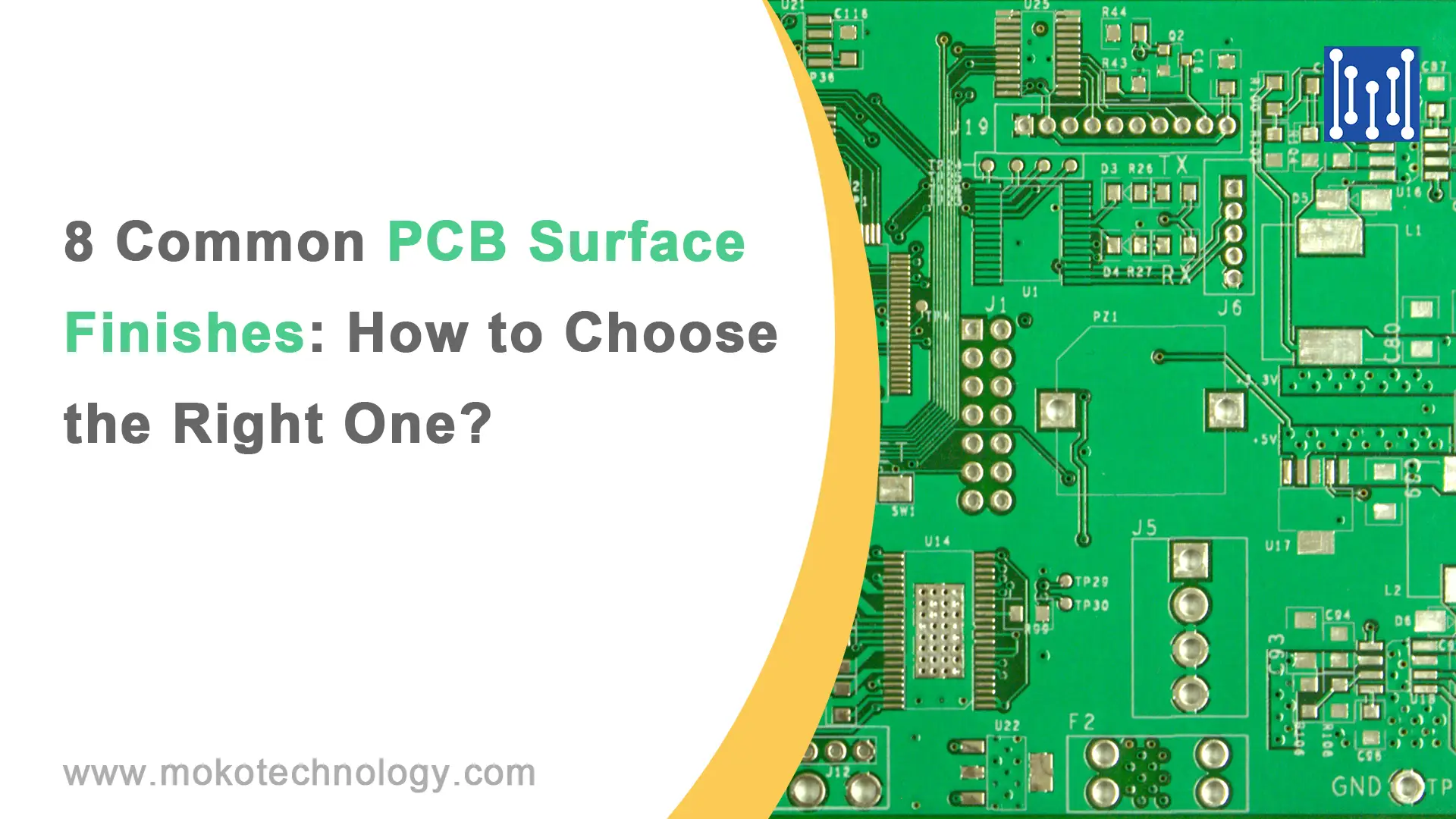
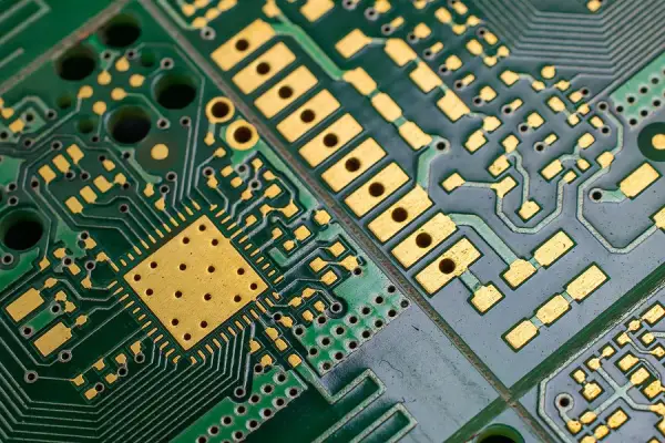
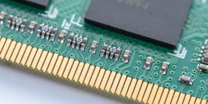
Bei der PCB-Oberflächenveredelung handelt es sich um eine Beschichtung oder Behandlung, die auf die freiliegenden Kupferleiterbahnen und -pads einer Leiterplatte aufgetragen wird. Es spielt eine entscheidende Rolle für die Funktionalität und Lebensdauer von Leiterplatten. This guide will overview 8 major PCB surface finishes including their advantages, limitations and applications. Zusätzlich, we list key considerations for selecting the right PCB surface treatment for your boards. Lesen wir weiter.
Why PCB Surface Finish Is Necessary?
Applying PCB surface finishes in Leiterplattenherstellung is crucial to safeguard copper traces from oxidation and environmental contaminants that degrade performance. These PCB surface finishes protect against moisture, Staub, Chemikalien, und extreme Temperaturen, preventing penetration and corrosion of the PCB-Material. They also aid in effective soldering and adhesion during assembly, enhancing thermal and electrical conductivity for better circuit efficiency. The right finish extends a PCB’s lifespan by reducing abrasion, preventing tarnish buildup, and resisting dendrite development that could cause shorts. Insgesamt, surface finishes are essential in both manufacturing and functionality, preserving solderability, limiting environmental damage, and ensuring smooth fabrication for specific applications.
8 Types of PCB Surface Finishes
-
HASL
Hot air solder leveling (HASL) is one of the most common PCB surface finishes because of its low cost and ability to be soldered. The HASL process involves dipping the PCB in liquid solder, then using hot air knives to level out the surface. While inexpensive and accessible, HASL has some limitations. The uneven topography can cause issues with small Oberflächenmontagekomponenten unter 0805 package size or fine pitch BGAs(ball grid arrays). Bridging between pads is also a risk on high density interconnect boards. Außerdem, standard tin-lead HASL contains lead, so it does not comply with RoHS regulations. Lead-free HASL is an option but comes at a higher cost.
For boards with mainly through-hole parts or large surface mounts, HASL remains a good economical choice. Yet for boards with ultra-fine pitch components, dense routing, and lead-free requirements, other finishes may be preferable.
-
Lead Free HASL
Lead-free hot air solder leveling (HASL) uses tin-copper, tin-nickel, or tin-copper-nickel alloys rather than standard tin-lead solder. This makes it an economical RoHS-compliant option. jedoch, like traditional HASL, it still suffers from uneven topography that can cause issues with small surface mounts.
For boards with high density finer pitch components, immersion coatings may be a better choice despite their slightly higher cost. The uniform deposition provided by immersion finishes helps prevent bridging and other defects on boards with tiny chip components or ball grid arrays.
Allgemein, lead-free HASL offers cost-effective solderability combined with regulatory compliance. Yet certain applications with small package sizes or fine feature sizes may benefit from the improved surface evenness of immersion finishes.
-
STIMMEN
Electroless gold over nickel (STIMMEN) is a pcb surface treatment that consists of a nickel plating layer covered by a thin gold layer. This combination provides a durable, corrosion resistant finish with an extended shelf life spanning years.
The immersion deposition process creates a uniform flat surface well-suited for boards with fine pitch Komponenten, BGAs, and small chip packages. ENIG also enables wire bonding. jedoch, it comes at a premium cost versus other finishes.
Potential issues to be aware of with ENIG are black pad formation under BGA packages and aggressive etching of solder mask, which may require larger mask dams. Fully solder mask defined BGAs should also be avoided with this finish.
-
ENEPIG
Electroless nickel electroless palladium immersion gold (ENEPIG) is a multilayer PCB surface finish that was first introduced in the 1990s. It consists of successive platings of nickel, palladium, and gold. While initially not widely adopted due to the high cost of palladium, ENEPIG has seen renewed interest in recent years.
This finish offers solderability comparable to finishes like ENIG and immersion silver, along with excellent corrosion resistance and extended shelf life exceeding 12 months. The uniform metal deposition provides a flat surface finish ideal for boards with high density components and fine feature sizes. ENEPIG is also wire bondable.
Potential drawbacks are still a higher cost than other common finishes and some limitations on reworkability. Compatibility with manufacturing processes also requires consideration. jedoch, for boards requiring shelf life, bondability, and solderability, ENEPIG may merit consideration despite its cost premium.
-
Hard Gold
Hard gold plating is one of the most durable PCB finishes, with typical thicknesses of 30-50 microinches of gold deposited over 100 microinches of nickel. It provides excellent wear resistance for components with frequent mating cycles like connectors. jedoch, hard gold is also one of the most costly finishes.
Because of its limited soldering capability, hard gold finds infrequent application in solder joints. Typical applications include edge connectors, battery contacts, and test points on prototype boards. The hardness and longevity make it well-suited for these use cases despite the high cost.
Advantages of hard gold plating are long functional lifetime, lead-free compatibility, und Korrosionsbeständigkeit. Disadvantages include the premium price and additional processing steps often required like bus plating.
-
Immersion Silver
Immersion silver is a lead-free PCB finish that does not oxidize copper like tin-based finishes. Noch, exposure to air often leads to its tarnishing. To preserve solderability, immersion silver PCBs require protective packaging and have a short shelf life of 6-12 months. Once removed from packaging, boards should undergo soldering within a day before the finish degrades.
The immersion deposition process creates excellent surface flatness for boards with fine pitch components or ball grid arrays. Immersion silver is also cost-effective relative to gold-based finishes. jedoch, handling and exposure risks mean assemblers must work quickly once boards are unpacked. Peelable masks should be avoided to prevent finish damage.
-
Immersion Tin
Immersion tin, a lead-free surface finish for PCBs, is implemented using a chemical deposition technique. It provides a thin uniform coating of tin over the copper traces. The flat topography of immersion tin makes it well-suited for boards with fine pitch components, ball grid arrays, and other small surface mounts. As an economical immersion coating, tin does have drawbacks. It can oxidize over time, lowering solderability. To ensure quality solder joints, assembly should follow within 30 days of plating. High volume production can mitigate this, but lower volumes may warrant a more shelf-stable finish like immersion silver instead.
Careful handling is required as immersion tin is sensitive to contamination and whisker growth risks. It also etches solder mask and limits use of peelable masks. jedoch, for cost-sensitive leaded or lead-free boards with prompt assembly, immersion tin can provide reliable solderability.
-
OSP
Organic solderability preservatives (OSPs) protect copper surfaces on printed circuit boards by depositing a thin organic coating. This OSP layer is applied through an automated process like dipping or spraying. It prevents copper oxidation prior to soldering.
OSP films are very thin, in the range of 0.05 zu 0.2 Mikrometer, so thickness cannot be directly measured. They provide temporary protection with a typical shelf life of 3-6 months. Compared to metallic finishes, OSPs have minimal environmental impact. jedoch, they require careful handling to avoid coating damage.
Advantages of OSPs include low cost, simple process addition, reworkability, and lead-free compatibility. Drawbacks are the short shelf life, inability to protect plated through holes, and potential issues with automated optical inspection.
Comparison Table of PCB Surface Finishes
After understanding the details of each surface finish, the following table provides a side-by-side comparison of their key attributes:
| Oberflächenfinish | Kosten | Haltbarkeit | Lötbarkeit | Ebenheit | RoHS-Konformität | Haltbarkeit |
| HASL | Niedrig | Mittel | Good for large parts | Uneven | Nein (for leaded HASL) | Mäßig |
| Lead-Free HASL | Low-Medium | Mittel | Good for large parts | Uneven | Ja | Mäßig |
| STIMMEN | Hoch | Lang (Jahre) | Exzellent | Very flat | Ja | Hoch |
| ENEPIG | Very High | Lang (12+ months) | Exzellent | Very flat | Ja | Very High |
| Hard Gold | Very High | Very Long | Begrenzt | Flat | Ja | Extremely High |
| Immersion Silver | Mittel | Short (6-12 months) | Exzellent | Flat | Ja | Mäßig |
| Immersion Tin | Low-Medium | Short (30 Tage) | Exzellent | Flat | Ja | Niedrig |
| OSP | Sehr niedrig | Short (3-6 months) | Gut (temporary) | Flat | Ja | Niedrig |
How to Choose the Right Surface Finish for Your PCB?
Below we list several key considerations when selecting printed circuit board surface finish for your PCB project:
Lötbarkeit – The ability of the finish to be wetted by solder during assembly, is important for ensuring good solder joint reliability.
Haltbarkeit – It refers to how long the finish can maintain solderability before oxidation occurs., which is crucial for preserving PCBs over extended periods.
Thermal Cycling Performance -The surface finish should be able to withstand repeated heating and cooling cycles during operation without cracking or degrading. This is important for products that will undergo temperature fluctuations and thermal stresses in their intended environment.
Wear Resistance – The ideal surface finish will resist wearing off or degrading during handling, Versammlung, mating of connectors, or other mechanical processes.
Kosten – The material and processing costs can vary substantially for different surface finishes, so the budget needs to be balanced with the performance requirements.
Lead-free Compatibility – If lead-free solder alloys will be used, the surface finish must be compatible with and wettable by lead-free solders.
Environmental Regulations – The surface finish must comply with any legislative restrictions on use of hazardous substances, such as the RoHS directive in Europe.
Letzte Worte
Selecting the best PCB surface finish for your product involves evaluating multiple factors. If you’re still contemplating the ideal PCB surface finish for your next project, erreichen Sie uns. We’ll assist you in making the right choice. With nearly two decades of experience manufacturing PCBs for leading technology brands across diverse industries worldwide, our company has developed substantial proficiency in PCB fabrication and assembly, utilizing a wide range of surface finishing techniques.