For those new to electronics design and manufacturing, the term “bare PCB” may sound confusing or vague. In this beginner’s guide, we will lift the veil on this fundamental component by clearly defining what a bare PCB is, discussing the major benefits it provides, and exploring the different testing methods used to validate these blank PCB boards. So let’s get started unraveling the mystery of this essential electronic building block!
What Is a Bare PCB?
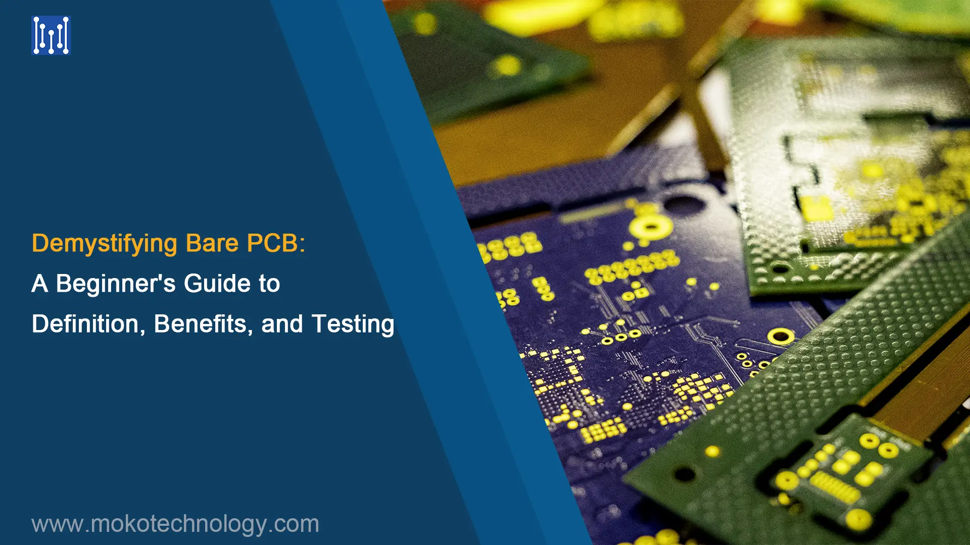
A bare PCB, also known as a blank circuit board, is a board that contains only the substrate, a metal coating, and the conductive pathways that connect the components. In contrast to a finished circuit board, a bare PCB lacks any installed components or circuitry. The board itself forms the core framework, featuring conductive traces etched or printed onto the substrate. Engineers and manufacturers depend on a bare PCB to kick things off when putting together a fully functioning circuit board. A bare PCB is the foundational base of a fully assembled PCB, providing the necessary structure before electronic components are added.
Materials Used for Bare PCB Manufacturing
Several key materials are used in crafting bare printed circuit boards. Some core options include:
- Polytetrafluoroethylene (PTFE)
Often called by its brand name Teflon, PTFE is valued for fabrication due to its mechanical strength, thermal resilience, and non-stick properties. This plastic withstands high temperatures and weather without losing structure or adhesion.
- Flame Retardant Type 4 (FR-4)
This glass-reinforced epoxy laminate offers flame resistance along with electrical and thermal insulation. The glass fiber boosts rigidity while the epoxy provides a smooth surface for etching copper traces. The “4” designation indicates the specific resin formulation.
- Metals
Copper proves the most common metal for conductive PCB traces and pads. This affordable material also exhibits excellent conductivity and ductility for etching precision paths. Other metals like aluminum or iron may be used as substrate backings or stiffening layers.
Further reading- A Must Read: PCB Material Guide
Benefits and Drawbacks of Bare PCB Board
Benefits
Early detection of design flaws – Because a bare PCB lacks any components or circuitry, the board layout, trace routing, and physical structure can be thoroughly inspected and tested. Engineers can identify potential issues with the board itself before proceeding with full assembly. For example, they may spot crosstalk problems, impedance mismatches, or errors in PCB trace connections. Finding and fixing these types of issues early prevents costly rework down the line.
Cost saving – When flaws in the board design are caught early using a bare PCB prototype, circuit board components do not need to be soldered onto defective boards. The cost of materials and labor for populating a full PCB is high. Identifying errors while the board is bare avoids wasting money assembling known faulty boards. The cost of reworking or scrapping assembled PCBs is far more than fixing a bare board.
Time saving – Testing and debugging a populated circuit board takes much longer than inspecting traces on a bare board. Assembling components also extends the production timeline versus evaluating a blank PCB. Catching physical PCB errors early therefore prevents significant delays in getting a working board. Assembly and testing go smoother when issues are resolved with the bare board upfront.
Streamlined production – Once the bare PCB design is validated, the assembly process can proceed smoothly without backtracking. Manufacturing fully populated boards is optimized when problems are ironed out in the prototyping stage on a bare board. This makes the full production ramp up faster and more efficient.
Drawbacks
Still prone to some errors – While easier to inspect, bare PCBs can still have small physical defects. These include over-etched copper, holes drilled slightly off target, spots with insufficient solder mask, and other flaws. Thorough examination and testing is required to catch all potential mistakes.
Limited testing capabilities – Electrical functionality cannot be completely validated without soldered components and circuits. A bare board can only test the physical layout and connections. Complete operation requires assembly of a populated board.
Additional initial stage – Creating bare PCB prototypes adds a preliminary step compared to directly assembling final boards. This front-end stage requires extra resources, time, and cost for the initial bare boards. However, this investment prevents much greater expenses from assembling defective boards down the line.
What Are Bare PCB Boards Used For?
Bare printed circuit boards provide the fundamental base for assembling a wide range of electronic devices and systems. From consumer gadgets to industrial equipment, bare PCBs are essential components that enable prototyping, testing, and production.
These blank canvas boards allow engineers to configure and optimize circuit board designs before attaching expensive electronic components. Bare PCBs offer mechanical support, conductive traces, and connection points to mount all other parts.
Using bare PCBs for early prototyping and testing helps identify potential issues with the board layout and fabrication. Catching flaws at this preliminary stage prevents problems down the line once fully populated boards are manufactured. The ability to validate designs upfront makes bare boards invaluable for streamlining development and production workflows.
Applications using bare PCBs span consumer devices, automotive systems, aerospace technologies, telecommunications infrastructure, medical equipment, green energy products, scientific instrumentation, and more. Any electronics needing custom circuit boards depend on bare PCB boards as the starting point for assembly and manufacturing.
Bare Printed Circuit Board Testing
Examining an unpopulated printed circuit board allows validation of the board’s intended electrical performance prior to component assembly. This preliminary bare board testing focuses on evaluating continuity and isolation across the traced connections.
Continuity testing verifies that the copper traces form complete circuits without gaps that would impede current flow. Meanwhile, isolation testing measures the resistance between distinct conductors to prevent shorting between circuits. Together, these tests validate that the physical board matches the design for proper functionality.
Types of Bare PCB Testing
Pinned Fixture – This technique uses an array of spring-loaded pins to simultaneously test all conductive points on the board. Custom fixtures apply pressure so the pins connect with top and bottom surfaces. Testing thousands of nodes at once enables efficient and rapid validation.
Flying Probe – Robotic arms with pointed probes move across the PCB to validate connections per programmed instructions. Although slower than a fixture, flying probes offer flexible testing for prototyping and small volumes.
Further Reading: PCB Flying Probe Test: What Is It? How It Works?
Automated Optical Inspection – Cameras photograph the blank board and compare it to schematics using image processing software. Discrepancies can be flagged for technicians to inspect visually. Adds rapid feedback but still requires electrical tests.
Burn-in Testing – Operating the bare board for extended periods under high temperatures and voltages stresses components to uncover latent defects. This intense testing method can destroy boards but detects flaws before product release.
X-ray Imaging – Radiographic scanning identifies issues like poor solder joints or barrel cracks that may be hidden internally. However, x-rays only supplement electrical and performance validation.
Final Thoughts
In closing, bare printed circuit boards provide the critical starting point for electronics design and manufacturing across countless applications. Whether used for early prototyping, design verification, or establishing manufacturing workflows, the blank PCB forms the backbone of any custom electronic system. By understanding what comprises a bare board, how it enables testing and flexibility, and the methods used to validate quality, the foundational role of bare PCBs becomes clear. While the manufacturing process is complex, partnering with an experienced PCB company simplifies tapping into these benefits. For nearly 20 years, MOKO Technology has delivered reliable, high-quality PCB solutions ranging from bare boards to full PCBA assembly. Our expertise produces optimized bare PCBs to meet diverse application needs. Whether you need simple blank boards or complex multilayer designs, MOKO has the capabilities required. Contact us today to get an instant quote!