- You can get a soldermask-like material in a small touch-up bottle.
- Maybe you cancut the pad with a razor just to make some space.
- Getting bridging during the reflow process.
Read More: PCB Design and Layout
#PCB Design
Read More: PCB Design and Layout
#PCB Design
Our brand was focused on common electronic product with single PCB. And this year, we plan to develop a smart range which may require multiple layer PCB. Want to know more about 2 layer PCB or 4 layer PCB.
I required a BOM from PCB designer of manufacturer, but he sent me a Gerber. How can I open and read it?
I am getting a PCB manufactured for a project that I am working on. One of the parts, the A4950 motor driver, has a “pad” on the bottom, which is meant to be soldered to GND of the PCB for thermal dissipation. I was thinking about the prototyping, and I am unsure how I would go about (using a soldering iron), soldering the pad on the bottom.
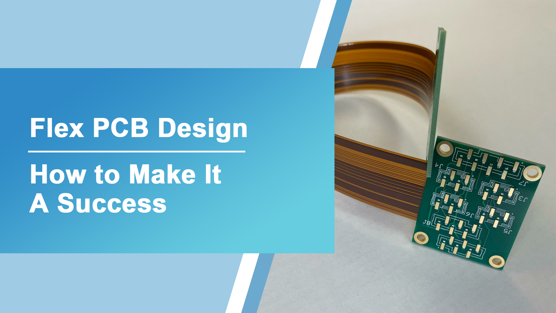
Flex PCBs, or Flexible Printed Circuit Boards, have gained significant popularity in recent years due to their unique properties and advantages in various applications. These
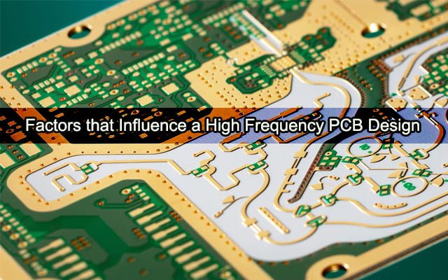
You are here because you want to learn about high frequency PCB design. This guide explains in detail different factors having an influence on high
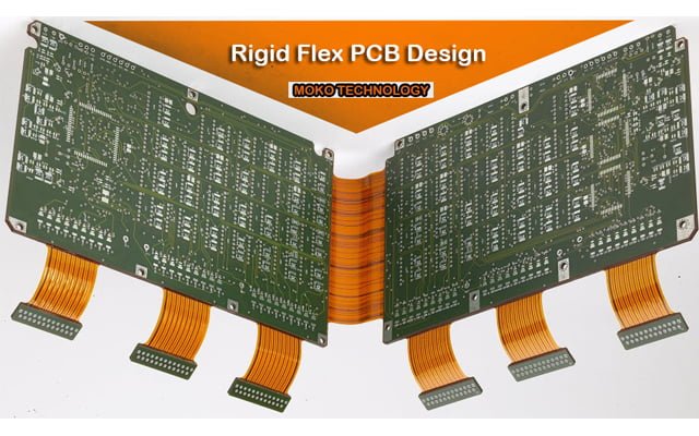
Rigid Flex PCB Design: Benefits and Design Best Practices With the use of a rigid flex PCB(rigid FPC), flexible circuit substrates and rigid circuit substrates
Electronic Manufacturing
Resources
Contact Us
Copyright ©2024 MOKO Technology | Your Trusted EMS Partner 粤ICP备15085690号