Bluetooth is everywhere these days! You can find it in smartphones, headphones, speakers – pretty much any gadget that connects wirelessly likely uses Bluetooth. So when building a new electronic product that needs wireless functionality, adding Bluetooth usually makes sense. To make that happen, you typically need a custom-designed Bluetooth circuit board. In this blog post, we’ll provide guidance on effective Bluetooth PCB Board design. To begin, we’ll introduce fundamental knowledge about Bluetooth circuit boards.
Understanding Bluetooth Circuit Boards
First, let’s review how Bluetooth technology works. Bluetooth leverages radio frequencies to enable communication between devices. Operating at 2.4 GHz, it can enable wireless connections similar to other standards like Wi-Fi. The effective range spans from 1 centimeter out to 100 meters. An important aspect of Bluetooth is that devices must pair and establish an authorized unique code before being able to exchange information. Additionally, Bluetooth-equipped hardware can conserve energy by entering standby mode when not actively transmitting data.
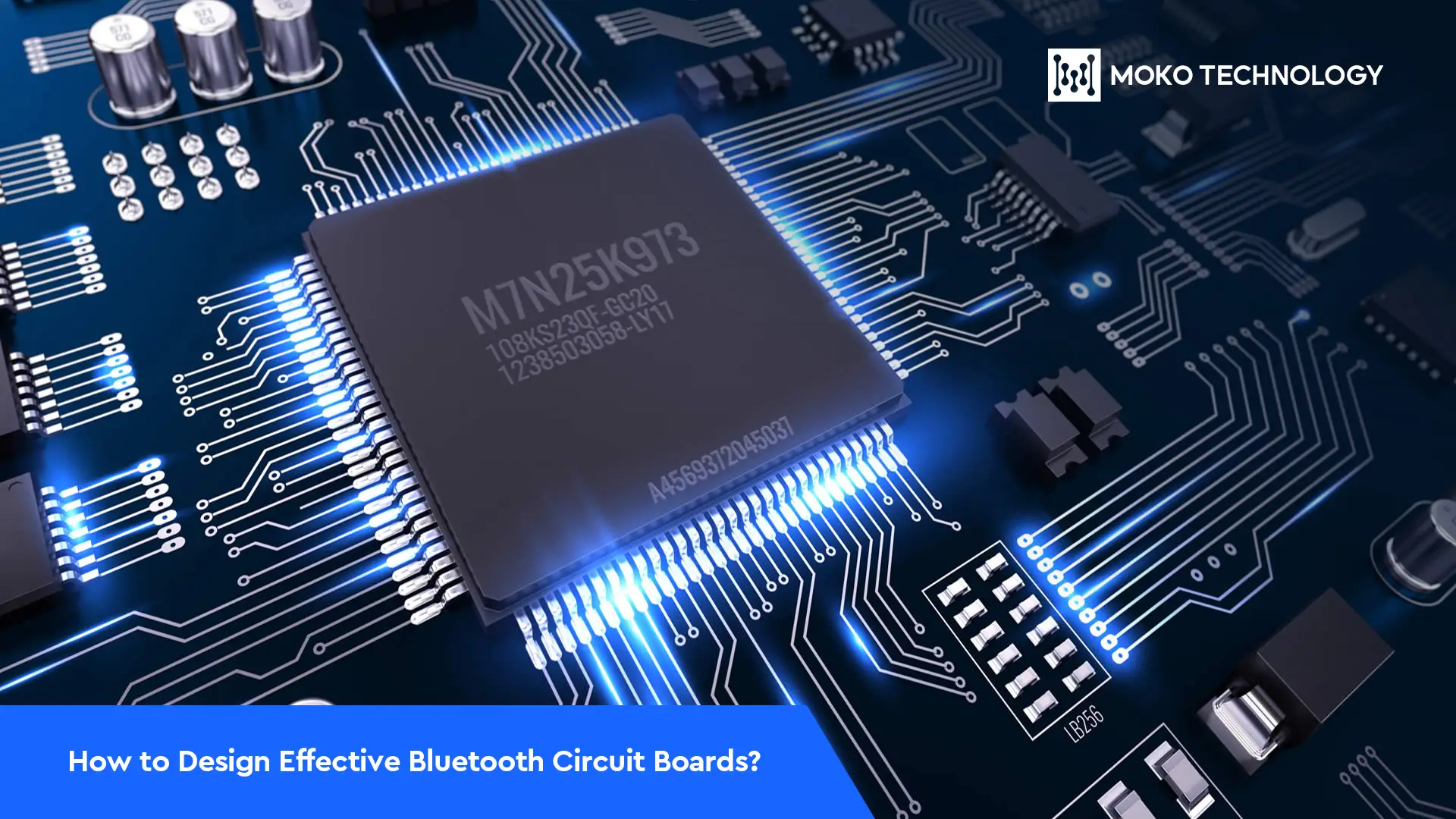
A Bluetooth PCB board refers specifically to the printed circuit board that enables Bluetooth capabilities. It contains a Bluetooth module or chip, an antenna for transmitting/receiving signals, a microcontroller to process wireless data, and supporting components like capacitors, resistors, and transistors. The Bluetooth module contains the radio transceiver along with a baseband controller, protocol stack, interface firmware, and more. Quality antenna placement on the PCB ensures good wireless range between connected devices. Careful circuit design is needed to manage power consumption while maintaining the bandwidth for data throughput speeds expected by the application.
Applications of Bluetooth Circuit Boards
Bluetooth technology enables wireless connectivity for a vast range of applications, including:
- Retail beacons for location sensing
- Industrial sensor data collection
- Audio products like wireless headsets
- Gaming controllers and computer peripherals
- Home automation control systems
- Cameras, printers, phones and consumer electronics
While leveraging the same core Bluetooth protocol, the implementation and optimization vary significantly across these applications depending on the use case data rates, connectivity modes, operating range, and reliability demands.
Compared to Wi-Fi, Bluetooth offers lower peak speeds and more limited range, especially through walls or other obstructions. However, version 5.0 brings improved throughput over prior releases. Importantly, Bluetooth maintains relatively low power draw, security protections, support for small peripheral devices, and widespread compatibility.
When developing a Bluetooth-enabled PCB, engineers make various design decisions to strengthen signal integrity and minimize interference/packet loss for their application. Next, we’ll provide some insights to optimize the performance of Bluetooth circuit boards.
Considerations and Tips for Bluetooth PCB Board Design
- Use Certified Modules
Using a pre-certified Bluetooth module from vendors like Microchip or Silicon Labs simplifies integration by packing in the Bluetooth radio, tuned antenna, firmware stack, and microcontroller into a self-contained solution. Modules undergo required testing and certification with regulatory bodies to save engineering teams’ effort. They allow faster time-to-market by eliminating complex RF layouts and antenna tuning. Common certified modules feature integrated ARM processors to handle Bluetooth communications and control I/O peripherals over GPIOs, SPI, I2C, and PWM pins.
- Carefully Position Antenna
The antenna enabling wireless connectivity must be carefully positioned on the edge of the board, enclosed in a plastic RF compartment when possible. Any nearby copper planes, PCB traces, pads, or polygon pours can degrade RF performance which is why Bluetooth chip vendors provide detailed layout guidelines. These require clearance areas on layers above and below the antenna section out to solder mask edges. Vias stitching signal layers to the ground help contain radiation. Shaping the board to place a Bluetooth antenna at one end or corner separates it from other electronics.
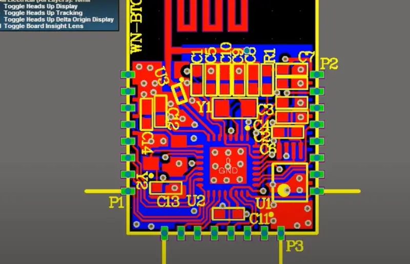
- Interference Mitigation
With Bluetooth utilizing the crowded 2.4GHz frequency band, interference from other wireless signals can disrupt connectivity and lower data speeds. Sources include WiFi routers, Zigbee devices, microwaves, wireless video equipment, and more sharing the same frequencies. Carefully consider the environment the Bluetooth PCB will operate in, and where possible position the board away from known interfering radios. Additional shielding around the antenna, noise-filtering components, and software techniques can help mitigate interference issues.
- Power Consumption
Bluetooth was designed to be lower power than WiFi, but still must be optimized for acceptable battery runtime. Develop detailed system power budgets estimating usage modes, transmit/receive cycles, idle listening time, and so on. Select lower power Bluetooth modules and microcontrollers, utilize power saving sleep modes between data transmissions, minimize activity timing, and similar techniques to extend operation on a single charge. The PCB design should avoid leakage paths and ensure stable clean power is delivered to Bluetooth components.
- Physical size constraints
When designing a Bluetooth PCB device that needs to be portable, physical size limitations must be considered. The enclosure the device will fit into imposes constraints on the overall PCB size. Additionally, because the device likely needs to incorporate components to perform other functions beyond Bluetooth connectivity, the PCB’s space needs to be carefully managed. Carefully choosing chip package sizes and positions can help optimize the use of the available space.
- Consider Real-World Interferences
Everyday materials like water and metal objects easily obstruct Bluetooth radio waves, even at short 1-2 meter distances. Microwaves, WiFi, and other consumer electronics congest the 2.4GHz band. Enclosing antennas in metal shields further degrades connectivity. Expect an inverse distance signal loss squared relationship. To compensate, utilize a higher gain antenna or lower data rates. Testing prototypes in real operating environments determines necessary interference mitigations.
- Testing & Certification
Vigorously testing the Bluetooth PCB design under a diverse range of operating environments and use conditions is vital—before deploying it to production. Test different positions and orientations for the board and external interfering sources to qualify wireless range and throughput. Ensure compatibility with target device software stacks and operating systems during integration. Finally, submit to Bluetooth SIG for full qualification and branding for end products.
Further reading: Why the PCB Testing is Necessary?
Conclusion
Bluetooth wireless technology continues advancing to empower ever more embedded applications and devices. Integrating Bluetooth connectivity introduces hardware and software design intricacies for the best performance, from component selection to antenna placement to interference mitigation. Following guidance on certified modules, antenna isolation, power optimization, environmental reliability testing, and final certification creates an effective development process. With these insights on key considerations when designing Bluetooth circuit boards, engineers can fully leverage Bluetooth capabilities for reliable wireless control, communication, updates, and more in their next-generation products.
