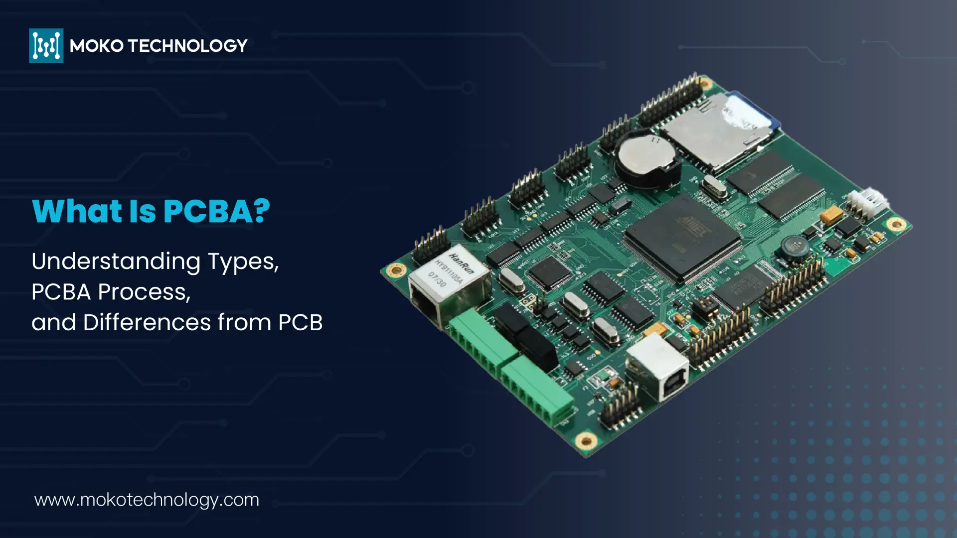
PCBA(Printed Circuit Board Assembly) stands at the heart of modern electronic devices, all the compact, efficient, and reliable electronic products we use today rely on it. But for some novices, they don’t know much about PCBA, so we decided to write an article like this to comprehensively introduce PCBA including its types, production process, PCBA testing methods, etc. Let’s get started with its definition.
What Is PCBA?
PCBA refers to the finished board after all the electronic components are soldered onto a printed circuit board (PCB). And we call the process of assembling components on the circuit board as PCB Assembly, which plays a very significant role in the manufacturing of electronic devices. The main purpose of a PCBA is to act as a platform that supports the necessary electronic components to work harmoniously, so as to achieve the intended functions of the electronic device.
Types of PCBAs
According to the assembly techniques, we can divide PCBAs into 3 types: SMT PCBAs, through-hole assembled PCBAs, and mixed-technology PCBAs.
-
SMT PCBA
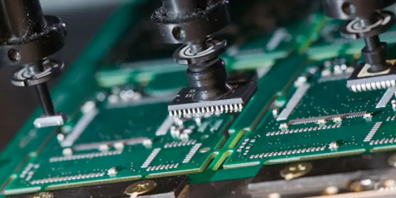
SMT PCBAs, as the name suggests, use surface mount technology where the components are mounted directly onto the PCB and connected to the traces through reflow soldering. SMT components are comparatively small and can be assembled on both sides of the PCB to achieve compact designs. PCBAs with surface mount assembled parts are used in most electronic products due to their enhanced performance and the ability to save space. And BGA assembly is particularly important for high-density connections in applications such as processors and memory chips.
-
Through-hole assembled PCBAs
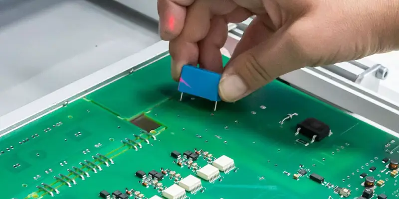
Through-hole assembled PCBAs refer to printed circuit boards where electronic components are mounted using the through-hole technology. In this assembly method, components have leads that are passed through holes drilled through the PCB and soldered on the other side. This assembly technique comes with benefits such as improved mechanical joints and fast prototyping. However, they are not suitable for small and dense PCB designs as through-hole components are relatively larger in size than the Surface Mount Devices (SMDs).
-
Mixed-technology Printed Circuit Board Assembly
In mixed-technology printed circuit board assembly, through-hole and surface mount components are used on the same board. This kind of PCBA capitalizes on the benefits associated with both through-hole and surface mount techniques of assembly. It is usually applied where the design involves the usage of through hole connection which is mechanically secure and surface mount technology which affords density.
Differences between PCBA and PCB
PCB and PCBA are two terms that look very similar, and beginners in the electronic industry often feel confused about them. So what’s the difference between PCB and PCBA?
A PCB serves as the foundational platform, comprising the non-conductive substrate and conductive pathways that electrically connect various components, but without any electronic components attached. It is essentially a blank board waiting for the addition of components. PCBA, on the other hand, represents the next step in the manufacturing process, where electronic components like resistors, capacitors, and integrated circuits(ICs) are soldered onto the PCB, making it a fully assembled and functional circuit board ready for use in electronic devices.
Below we have listed a table that lists the main differences between PCB and PCBA:
| Feature | PCB | PCBA |
| Definition | Bare board with conductive tracks | Completed board with components |
| Components | No components attached | Components soldered onto the board |
| Functionality | Cannot function on its own | Ready for use in electronic devices |
| Complexity | Simpler | More complex |
| Cost | Lower | Higher (includes components and assembly) |
| Testing | Basic electrical tests | Functional and quality tests |
| Time to produce | Shorter | Longer (includes assembly time) |
PCBA Process: A Step-by-Step Guide
The PCBA process involves several crucial steps to assemble a functional printed circuit board:
- Solder Paste Stenciling:The process starts with the deposition of solder paste on specific areas on the circuit board where components will be soldered. This paste is a composition of tin balls mostly but contains a little silver and copper together with the flux that aids in melting and fixing on the board.
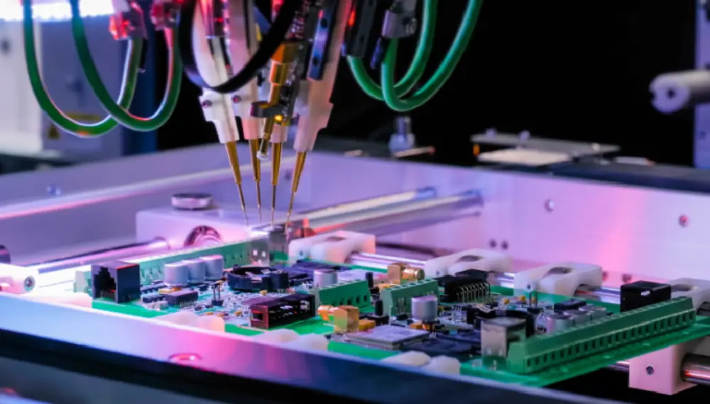
- Pick and Place: Electronic components and SMDs are placed onto the board using the manual tweezer and sometimes machines to place the components in the right position.
- Reflow Soldering: During the reflow soldering, the board is exposed to a conveyor belt of the oven which can reach up to 250°C where the solder paste melts and firms up the components on the board when it cools.
- Inspection and Quality Control: After reflow, inspection is performed to check if there are any connection defects or misconnections, making sure that all the leads are well and tightly soldered on the board.
- Insertion of Through-Hole Components: Some circuit boards also need to use through-hole components. These components require holes in the PCB to get signals from one layer to another. This step can be done by manual and by machine.
- Manual and Wave Soldering: Manual soldering is used for individual PTH component insertion, which is a time-consuming process. Another method is wave soldering where the board is passed over the molten solder and the components are fixed. Nonetheless, wave soldering is not friendly to use with double-sided PCBAs.
Further reading: Wave Soldering vs. Reflow Soldering: What’s the Difference? - Testing and Final Inspection: The last step involves a rigorous functional testing where a product is tested in real operating conditions: different options of Voltage, signals, currents, etc., in order to identify any problems that might occur.
Popular PCBA Testing Methods
- In-circuit testing (ICT):It is a commonly used testing technique involving the use of a bed of nail fixtures that contains multiple contact points to touch several points on the board all at once. This technique includes the identification of the presence, orientation, and basic operations of individual components. As much as ICT is fast and very efficient compared to others, it deals with the use of customized fixtures for each layout of the boards.
- Flying Probe Testing (FPT): In FPT, the probes are used in a movable manner to test various points on the board. Compared to ICT, it is more flexible because it doesn’t require custom fixtures. Nonetheless, FPT is relatively slower than ICT in mass-scale testing.
- Automated Optical Inspection (AOI): It is an equipment system that uses a high-resolution camera along with an image processor to look for defects in the circuit board like missing components, wrong component placements, and solder problems. AOI is an efficient and non-contact inspection, but sometimes it may miss internal or hidden flaws.
- Automated X-ray Inspection (AXI):In this testing method, X-rays are used in order to check internal aspects of components and solder joints. This method is particularly valuable in the assessment of BGAs (ball grid arrays) and other hidden connections. While AXI costs more than AOI, the range of inspection is much wider.
- Functional testing (FCT): It is conducted in order to assess the functionality of the board by mimicking the actual operating environment. FCT can be a very time-consuming process, which has to be done with custom test equipment. Event though, it is necessary as it ascertain that the board is operating as was designed to.
How to Choose the Best PCBA Manufacturer?
Choosing the best PCBA manufacturer is crucial to ensuring the quality and reliability of the products. Below we list key factors that should be considered when finding your PCBA manufacturing partner:
- Quality Assurance
The quality is always the primary concern. In selecting a PCBA manufacturer, we must consider if they meet the standard, if they have complied with a certification like ISO9001, and if they have a strict quality control system.
- Technical Proficiency
In order to work on your project, a PCBA manufacturer must be capable of meeting the specifications of your project. This comprises their skill in handling various technologies of the PCBA such as through-hole and surface-mount technologies; their ability to handle the various components and materials, and their manufacturing capabilities as well.
- Pricing
Though quality is crucial, one cannot overlook the cost factor in manufacturing the PCBA. It is always ideal for us to work with a PCBA manufacturer who provides affordable prices and quality products at the same time.
- Production Timeline
Another important consideration is the time that it takes to produce the PCBA. In this regard, it is essential to choose a manufacturer that is well capable of working within your time frame to deliver high-quality boards.
Work with MOKO Technology for Your PCBA Project Success
As a leading PCBA manufacturer in China, MOKO Technology is dedicated to delivering high-quality circuit boards at competitive prices, with a commitment to transparency and no hidden fees. We are proficient in different PCB assembly technologies, and our state-of-the-art facility is designed to accommodate the diverse needs of our clients. We have a stringent quality control process to ensure the quality of each product. Reach out to us to start your project now!
FAQs about Printed Circuit Board Assembly
What factors affect PCBA cost?
Major factors affecting PCBA cost include the size of the board, number of layers, complexity, number of components, volume of production, type of tests that need to be done, and the time it takes to complete. Higher complexity and shorter turnaround time usually lead to the higher cost.
What’s the difference between SMT and through-hole assembly?
SMT is the process that places components on the surface of the PCB while through-hole involves insertion of the components through drilled holes on the PCB and soldering on the other side of the board. The SMT enables a higher component density and the technique is more widely used in modern PCBAs.
Can I use both through-hole and surface-mount components on the same PCBA?
Yes, through-hole and surface-mount components can be used on the same PCBA, in this way, the PCBA benefits from the strong mechanical strength of through-hole and the high density of surface-mount technology.
What are common PCBA defects?
Some of the common defects are solder bridges, cold or dry solder joints, bad component position, missing components, wrong polarity, and components getting damaged due to heat during soldering.
How does MOKO Technology ensure the quality of Printed Circuit Board Assembly?
The quality control of MOKO Technology’s PCBA starts with careful designs. Also, we have a standardized production process and implement a series of testing methods to ensure the utmost quality of each board.
Can PCBAs be repaired if they fail?
In most cases, Yes, they can be repaired. However, some severely damaged PCBAs can not be repaired. Generally, repairing PCBAs involves replacing components, and fixing soldering issues or damaged traces.