HDI PCB
From PCB design to mass production, MOKO provides one-stop HDI PCB manufacturing services to help customers shorten time-to-market and save costs.
Your Trusted HDI PCB Manufacturing Partner
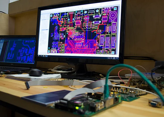
HDI PCB fabrication is rapidly becoming the ultimate solution for smaller, more efficient, and more durable PCBs. High-Density Interconnect (HDI) is a high-performance design that is characterized by its high density of components and routing Interconnections that use micro vias, blind and buried via or micro via techniques, and built-up Print Circuit Boards (PCBs) laminations.
As HDI PCBs specialist, MOKO Technology has extensive experience in manufacturing HDI PCBs for customers in different industries such as medical, automotive, and electronics. We have the ability to handle all HDI PCBs projects with unmatched accuracy and high quality within your budget.
Why Choose Us

High Quality
MOKO has a strict quality control system, we use various inspection methods to inspect each circuit board and even each component, working with us can save you from worrying about the quality.

Low Costs
We have a stable supply chain around the world, which enables us to get good materials at lower costs. In addition, all steps involved in HDI PCB manufacturing are completed under one roof which can save transportation costs.

Extensive Experience
We have been engaged in HDI PCBs manufacturing for about 17 years, serving customers from over 100 countries, our experienced engineers are well-versed in all types of circuit boards, and their expertise can ensure your project’s success.

Quick Delivery
Our one-stop manufacturing service allows us to better control the production schedule and deliver the HDI PCB within the time you require. In addition, we utilize industry-leading and highly automated equipment for production, which can significantly reduce manufacturing time.
Our HDI PCB Cases
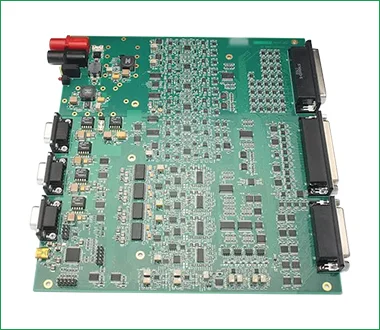
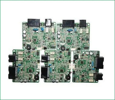
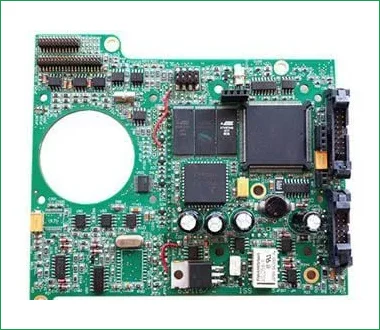
Our Certifications
MOKO has obtained many certifications including ISO9001:2015, ROHS, BSCI, IPC, and UL, which demonstrates our commitment to stringent PCB quality control.


HDI PCB Specification at MOKO Technology
HDI PCB Applications

HDI PCB FAQs
HDI PCB (High-Density Interconnect PCB) is a kind of printed circuit board with a higher wiring density per unit area with small size of via, thin width of trace and more concentration of components.
HDI PCBs provide benefits such as better signal integrity, smaller size, faster signal transmission, making them preferred in device with limited space and high performance.
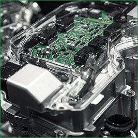
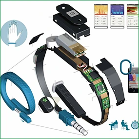
HDI PCBs are used in smart phones, tablets, medical equipment, wearables, aerospace applications, automotive electronics, and so on.
HDI PCBs have tighter line widths, smaller via holes and a higher number of connections as compared to the standard PCBs, making it possible to fit more complex designs in a comparatively smaller area.
HDI PCBs employ microvias, blind vies and buried via to make the entire size of the board smaller and to provide better connection between different layers.
Commonly used substrate materials in High-Density Interconnect PCBs are FR4 and polyimide.
Some of the challenges when designing the HDI PCBs are signal integrity, heat dissipation issues and problems associated with manufacturing constraint like smaller via and trace width.
Yes, high density interconnect PCBs can enhance the thermal management.Their compact design and efficient use of materials allows the heat to be dissipated fast even in high power applications.
We can fabricate types of HDI PCBs from simle single-layer HDI PCBs, multi-layer HDI PCBs to complex ones with stacked and staggered vias to meet different needs.
Yes, of course. Our flexible manufacturing capability allows us to handle different order volumes, from prototyping to low-volume and large-volume production runs.
Yes, MOKO Technology offers design for manufacturability (DFM) and design for testing (DFT) support.
MOKO Technology employs strict quality control measures and advanced testing techniques including Automated Optical Inspection (AOI), X-ray inspection, and electrical testing to ensure the highest quality.
